Once a year, during the TSMC’s Open Innovation Platform (OIP) Forum you can expect to see cutting edge technical achievements by TSMC and their partners. This year was no exception, with Open-Silicon presenting its accomplishments in implementing an HBM reference design in 16nm. It’s well understood that HBM offers huge benefits… Read More

Tag: cowos
Four Takeaways from the TSMC OIP 2015
Paul M. did an excellent job summarizing the technical information that TSMC presented at the recent Open Innovation Platform symposium. I’d like to also share an impression on four areas that struck me as key to TSMC’s strategy.… Read More
TSMC 10nm Readiness and 3DIC
At the TSMC Technology Symposium last month Suk Lee presented a lot of information on design enablement. Suk is an interesting guy with a unique background in ASIC, Semiconductor, EDA, and now Foundry. In baseball terms that would be like playing infield, outfield, home plate, and umpire!
Around the turn of the millennium Suk actually… Read More
TSMC Processes Galore
Today was TSMC’s 2015 North American Technology Symposium. They talked about a lot of things but perhaps the most important was that they gave a lot of details of new processes, new fabs, and volume ramps.… Read More
TSMC Delivers First FinFET ARM Based SoC!
Right on cue, TSMC announces 16nm FinFET production silicon. I believe this is the original version of FinFET versus 16FF+ which is due out in 1H 2015. I will confirm this next week at the TSMC OIP event in San Jose, absolutely. Either way this is excellent news for the fabless semiconductor ecosystem and I look forward to the first … Read More
Temperature – The Fourth Aspect to Look at in SoC Design
In my career in semiconductor industry, I can recall, in the beginning there was emphasis on design completion with automation as fast as possible. The primary considerations were area and speed of completion of a semiconductor design. Today, with unprecedented increase in multiple functions on the same chip and density of the… Read More
Smart Strategies for Efficient Testing of 3D-ICs
3D-IC has a stack of dies connected and packaged together, and therefore needs new testing strategies other than testing a single die. It’s given that a single defective die can render the whole of 3D-IC unusable, so each die in the stack must be completely and perfectly tested before its entry into that stack. Looking at it from a … Read More
TSMC: 3D, 450mm, CoWoS and More
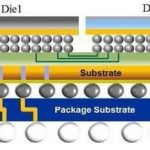
The first keynote at the Burlingame 3D conference was by Doug Yu of TSMC. Not surprisingly he was talking about 3D. In particular, TSMC has WLSI technology that they call CoWoS, which stands for chip-on-wafer-on-substrate which pretty much describes how it is built. This is the technology that Xilinx uses for its recently announced… Read More
Xilinx and TSMC: Volume Production of 3D Parts
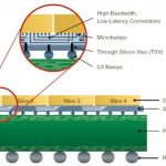
A couple of weeks ago, Xilinx and TSMC announced the production release of the Virtex-7 HT family, the industry’s first heterogeneous 3D ICs in production. With this milestone, all Xilinx 28nm 3D IC families are now in volume production. These 28nm devices were developed on TSMC’s Chip-on-Wafer-on-Substrate (CoWoS)… Read More
Double Patterning for IC Design, Extraction and Signoff
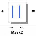
TSMC and Synopsys hosted a webinar in December on this topic of double patterning and how it impacts the IC extraction flow. The 20nm process node has IC layout geometries so closely spaced that the traditional optical-based lithography cannot be used, instead lower layers like Poly and Metal 1 require a new approach of using two… Read More