You are currently viewing SemiWiki as a guest which gives you limited access to the site. To view blog comments and experience other SemiWiki features you must be a registered member. Registration is fast, simple, and absolutely free so please,
join our community today!
If you don’t get the tongue in cheek reference of the title, you probably don’t have children who liked to watch Disney movies. All four of my daughters loved Disney and so, I am forever shaped by the Wonderful World of Disney. In 2007 Disney adapted to the screen a novel called, ‘A Bridge to Terabithia’, in which two adolescents escape… Read More
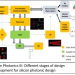
I cut my teeth in silicon IC design at Texas Instruments during the early 1980’s working on what would eventually become the ASIC and Fabless IC industries that enabled the explosive growth of the electronics industry over the last three decades. Of late I’ve become involved in the silicon photonics space and I am getting an incredible… Read More
The International Electron Devices Meeting (IEDM) is one of, if not the premier conference for semiconductor process technology. The 2015 meeting just finished up on Wednesday, December 9th.
This year’s meeting was held from Saturday, December 5[SUP]th[/SUP] through Wednesday, December 9[SUP]th[/SUP] in Washington DC.… Read More
The big picture is that planar semiconductor transistors don’t really work below 20nm. The reason is that the gate does a poor job of controlling the channel since too much channel is too far from the gate and so there is a lot of leakage even when the transistor is nominally off. So the channel needs to be made thinner. One way … Read More
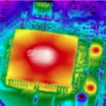
In the 1970’s we designed ICs first and when silicon came back then we measured the power and junction temperature. At that time there were no EDA simulation tools or models for full-chip power and temperature analysis. Fast forward to 2013 and we find that temperature and power are still demanding requirements for MPSoC … Read More
Grenoble is French city well-known within the Semiconductor industry to be one of the last location counting wafer fabs, not only in France but in fact in Europe. Back in the 70’s, under French government impulse, through the Commisariat à l’Energie Atomique (CEA) and the LETI subsidiary in charge of Electronic related research,… Read More