You are currently viewing SemiWiki as a guest which gives you limited access to the site. To view blog comments and experience other SemiWiki features you must be a registered member. Registration is fast, simple, and absolutely free so please,
join our community today!
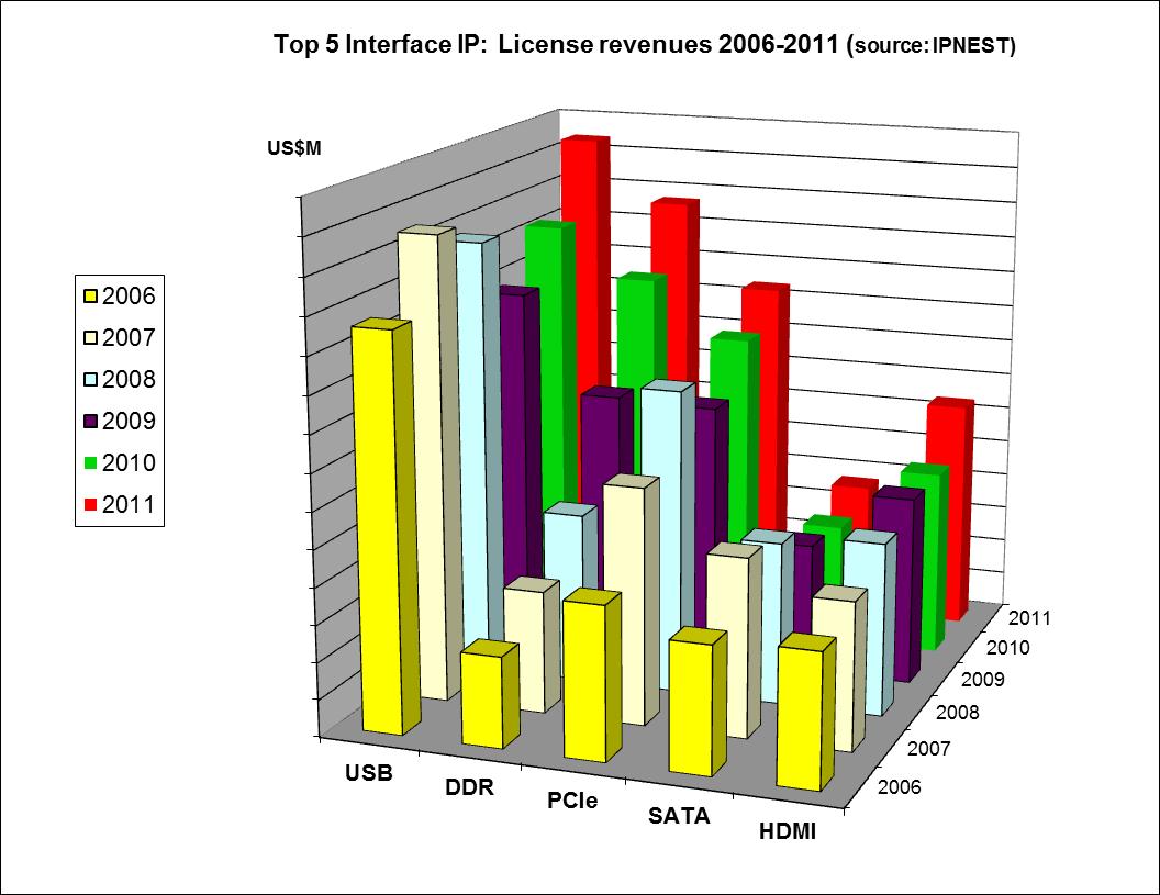
The industry is moving extremely fast to change the “old” way to interconnect devices using parallel bus, to the most efficient approach based on High Speed Serial Interconnect (HSSI) protocols. The use of HSSI has become the preferred solution compared with the use of parallel busses for new products developed … Read More
EDA software for IC and system design became a commercial business in the early 1980s. In those days, 3 companies – Daisy Systems, Mentor Graphics, and Valid Logic Systems – dominated the emerging EDA industry. However, two small startups that emerged in the early 1980s grew rapidly and merged to form Cadence Design Systems in 1988.… Read More
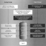
Last week I reviewed Chapter 1 in the new book: Mixed-Signal Methodology Guide, and today I finish up my review of Chapters 2 through 11. You can read the entire book chapter by chapter, or just jump directly to the chapters most related to your design role or project needs. With multiple authors I was impressed with the wide range of… Read More
Almost every SoC has multiple analog blocks so AMS methodology is an important topic to our growing electronics industry. Authored by Jess Chen (Qualcomm), Michael Henrie (Cliosoft), Monte Mar (Boeing) and Mladen Nizic (Cadence), the book is subtitled: Advanced Methodology for AMS IP and SoC Design, Verification and Implementation… Read More
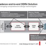
Cadence at 20nmby Paul McLellan on 08-21-2012 at 8:10 pmCategories: Cadence, EDA
Cadence has a new white paper out about the changes in IC design that are coming at 20nm. One thing is very clear: 20nm is not simply “more of the same”. All design, from basic standard cells up to huge SoCs has several new challenges to go along with all the old ones that we had at 45nm and 28nm.
I should emphasize that the paper… Read More
I was very happy to see that Cadence has decided to hold MEMCON again in 2012, in Santa Clara on September 18[SUP]th[/SUP] . The session will start with “New Memory Technologies and Disruptions in the Ecosystem”from Martin Lund.
Martin is the recently (March this year) appointed Senior VP for the SoC Realization Group at cadence:… Read More
Big processors get all the love, it seems. It’s natural, since they are highly complex beasts and need a lot of care and feeding in the EDA and fab cycle. But the law of large numbers is starting to shift energy in the direction of optimizing microcontrollers.
I mulled the math in my head for a while. In a world with 7 billion people and … Read More
I first met Brien Anderson on LinkedIn because we share common groups and interests, so I decided to interview him and discover how CAD tools enabled IC design at Synpatics, a company with capacitive sensing technology used in smart phones, tablets and touch screens.… Read More
A Brief History of EDAby Daniel Nenni on 08-05-2012 at 6:00 pmCategories: EDA
Electronic Design Automation, or more affectionately known as EDA, is a relatively young $5B industry with a very colorful upbringing, one that I have experienced firsthand, I’m very grateful for, and is an honor to write about. Today EDA employs an estimated 27,000 people! There is a nice EDA Wikipedia page which can be found here… Read More
I learn a lot these days through webinars and videos because IC design tools like schematic capture and custom layout are visually oriented. Today I watched a video presentation from Steve Lewis and Stacy Whiteman of Cadence that showed how Virtuoso 6.1.5 is used in a custom IC design flow:… Read More