You are currently viewing SemiWiki as a guest which gives you limited access to the site. To view blog comments and experience other SemiWiki features you must be a registered member. Registration is fast, simple, and absolutely free so please,
join our community today!
The TSMC quarterly conference call was last week and of course it stirred up quite a bit of controversy. Let me share with you my experience, observations, and opinions and maybe together we can come up with an accurate prediction for 2016. First let’s take a look at 20nm and what people now call the “Apple effect.”
Correct… Read More
For any semiconductor technology node to be adopted in actual semiconductor designs, the very first step is to have a Process Design Kit (PDK) developed for that particular technology node and qualified through several design tools used in the design flow. The development of PDK has not been easy; it’s a tedious, time consuming,… Read More
‘Laughing Buddha’ is eternal, but for semiconductor industry, I must say it’s ‘laughing Moore’. Moore made a predictive hypothesis and the whole world is inclined to let that continue, eternally? When we were at 28nm, we weren’t hoping to go beyond 20/22nm; voices like ‘Moore’s law is dead’ started emerging. Today, we are already… Read More
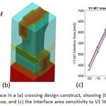
In the modern semiconductor ecosystem we are seeing rapid advancement in technology breaking past once perceived limits; 28nm, 20nm, 16-14nm, 10nm and we are foreseeing 7nm now. Double and multi-patterning are already being seen along with complex FinFET structures in transistors to gain the ultimate advantages in PPA from… Read More
Last month Cadenceannounced its fastest parasitic extraction tool (minimum 5 times better performance compared to other available tools) which can handle growing design sizes with interconnect explosion, number of parasitics and complexities at advanced process nodes including FinFETs, without impacting accuracy of … Read More
As I see the semiconductor industry going through significant changes and advances, yet ironically plagued by a growing perception that the pace of scaling is slowing, I was inclined to take a peek into what the industry experts say about the state of the industry and the future of Moore’s Law. Fortunately, at last week’s International… Read More
Engineers are always looking to improve the efficiency of how they work, but don’t want to sacrifice accuracy in the process. This is true in the world of semiconductor process development, where traditional build-and-test cycles are both time and resource intensive. But what if there was a way to do certain steps in a ‘virtual’… Read More