ASML reported results in line and slightly ahead of expectations which helped push ASML and the other semicap stocks back to their original valuations prior to the two step pull back that lasted about a month. We are now back to relatively high, record valuations not seen or ever seen previously (at least for a long time) by many companies.… Read More

Tag: asml
Standard Node Trend
I have previously published analysis’ converting leading edge logic processes to “standard nodes” and comparing standard nodes by company and time. Recently updated details on the 7nm process node have become available and in this article, I will revisit the standard node calculations and trends.… Read More
SPIE 2017 – ASML Interview and Presentations
At the SPIE Advanced Lithography conference I sat down with Mike Lercel, Director of Strategic Marketing for ASML for an update. ASML also presented several papers at the conference and I attended many of these. In this article, I will discuss my interview with Mike and summarize the ASML presentations.… Read More
SPIE 2017 ASML and Cadence EUV impact on place and route
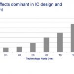
As feature sizes have shrunk, the semiconductor industry has moved from simple, single-exposure lithography solutions to increasingly complex resolution-enhancement techniques and multi-patterning. Where the design on a mask once matched the image that would be produced on the wafer, today the mask and resulting image … Read More
Intel Manufacturing Day: Nodes must die, but Moore’s Law lives!
Yesterday I attended Intel’s manufacturing day. This was the first manufacturing day Intel has held in three years and according to Intel their most in depth ever.
Nodes must die
I have written several articles comparing process technologies across the leading-edge logic producers – GLOBALFOUNDRIES, Intel, Samsung… Read More
An Steegen ISS Talk and Interview – Patterning Options for Advanced Nodes
At the ISS Conference in January, An Steegen EVP of Semiconductor Technology & Systems at imec gave a talk entitled “Patterning Options for Advanced Technology Nodes”. I was present for her talk and had the opportunity to have a follow up interview with An.… Read More
EUV is NOT Ready for 7nm!
The annual SPIE Advanced Lithography Conference kicked off last night with vendor sponsored networking events and such. SPIE is the international society for optics and photonics but this year SPIE Advanced Lithography is all about the highly anticipated EUV technology. Scotten Jones and I are at SPIE so expect more detailed… Read More
The post election Semicap bubble just burst in one day
Back to a more normal reality… Market gets”De-Fanged”… Where to from here? The “Icarus” Effect… Much of the market, and especially Tech & “FANG” (Facebook, Amazon, Netflix & Google) stocks gave back most all of their post election day gains in one session.… Read More
AMAT LRCX and EUV Economics
Lam & Applied talked about “sustainable” growth Both expect share gains & growth in a flattish market. We examine the “new, lower, cyclicality”. Although Applied and Lam are fierce competitors , coming at things from different directions, they sounded awfully similar last week.
… Read More
EUV transition comes into focus
We attended ASML’s analyst day in New York on Halloween. We were very impressed with the quality, content and clarity of the presentations and thought it was one of the best strategic positioning presentations we have seen in the semi industry. We also had an opportunity to meet with several members of senior management after… Read More