EDA industry pundit Gary Smithhas been talking about the electronics industry adopting an ESL tool flow for decades, so it was my pleasure to speak with Bill Neifertof Carbon Design Systemsat DAC this month because his company has been offering both tools and models that enable a virtual prototyping design flow.… Read More

Tag: asic
Semiconductor Cost Models: Boring But Crucial
One of the most important and underrated tasks in a semiconductor company is creating the cost model. This is needed in order to be able to price products, and is especially acute in an ASIC or foundry business where there is no sense of a market price because the customer and not the manufacturer owns the intellectual property and … Read More
Quoting Automatically the eSilicon Way
Every ASIC company has a major challenge: they have to work out what it is going to cost to build the customer’s product and commit to deliver it at that price. Too high and you lose the business. Too low and you will wish you’d lost the business. Historically this has been done largely manually. This is an expensive process.… Read More
ASICs for Bitcoin Mining!

One of the hottest areas for Application Specific Integrated Circuits today is Bitcoin mining. A good friend of mine has a son who is involved in a Bitcoin start-up so we have been discussing this at great length and I will share what I have learned thus far. Coincidently, my wife asked me about Bitcoin during our most recent walk down… Read More
A Brief History of TSMC OIP

The history of TSMC and its Open Innovation Platform (OIP) is, like almost everything in semiconductors, driven by the economics of semiconductor manufacturing. Of course ICs started 50 years ago at Fairchild (very close to where Google is headquartered today, these things go in circles). The planarization approach, whereby… Read More
Reliability sign-off has several aspects – One Solution
Here, I am talking about reliability of chip design in the context of electrical effects, not external factors like cosmic rays. So, the electrical factors that could affect reliability of chips could be excessive power dissipation, noise, EM (Electromigration), ESD (Electrostatic Discharge), substrate noise coupling and… Read More
The Funnest Bug

We all have a funnest bug we’ve been involved with. I don’t think ‘funnest’ is actually a word but when my kids used to use the word ‘funner’ I didn’t have a good argument as to why it wasn’t a word, it just seemed a word I’d never heard. In fact I have no idea what the rules are… Read More
A Brief History of VLSI Technology, part 2
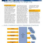
VLSI’s business grew healthily but it never threw off enough cash to fund all the investment required for process technology development and capital investment for a next generation fab. They made a strategic partnership with Hitachi covering both 1um process technology and a significant investment, which meant that … Read More
A Brief History of VLSI Technology, part 1
VLSI Technology was founded in 1981 by Dan Floyd, Jack Baletto and Gunnar Wetlesen who had worked together at Signetics. The initial investments were by Hambrecht and Quist, a cross between a VC and a bank, and by Evans and Sutherland, the simulation/graphics company.
The fourth person to join the company was Doug Fairbairn. He … Read More
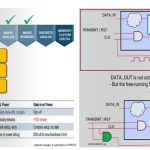
Full Visibility in ASIC Prototypes at DAC

ASIC prototyping from multiple vendors using FPGA boards was popular at DAC again this year in Austin, Texas. I stopped by the Tektronix booth for a few minutes to meet with Dave Orecchio to get an update.
Dave Orecchio (right), Tektronix… Read More