You are currently viewing SemiWiki as a guest which gives you limited access to the site. To view blog comments and experience other SemiWiki features you must be a registered member. Registration is fast, simple, and absolutely free so please,
join our community today!
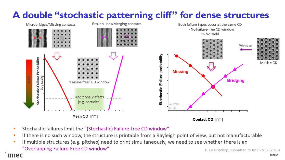
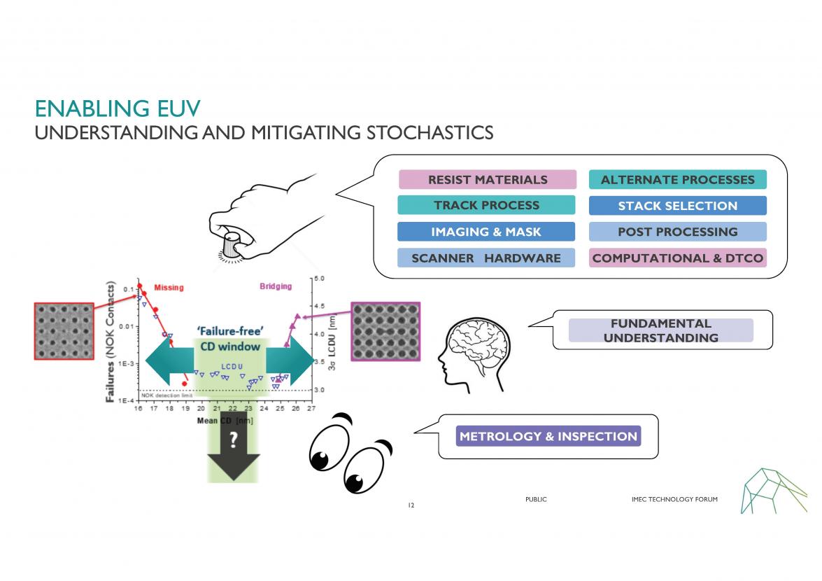
At the SPIE Advanced Lithography Conference Imec presented several papers on EUV and Veeco presented about etching for EUV masks. I had the opportunity to see the presentations and speak with some of the authors. In this article I will summarize the key issues around EUV based on this research.
EUV is ramping up into high volume 7nm… Read More
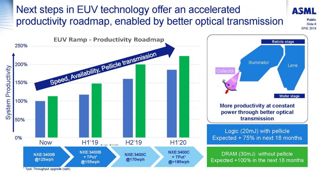
At the SPIE Advanced Lithography Conference ASML gave an update on both the current 0.33NA system and the 0.55 high-NA system development. I saw the presentations and got to sit down with Mike Lercel (Director of Strategic Marketing).… Read More
I was asked to present at Nikon’s LithoVision event again this year. LithoVision is held the day before the SPIE Advanced Lithography Conference also in San Jose. The following is a write up of my talk.… Read More
At SEMICON West I attended the imec technology forum, multiple Tech Spot presentations and conducted a number of interviews relevant to advanced lithography and EUV. In this article I will summarize what I learned plus make some comments on the outlook for EUV.… Read More
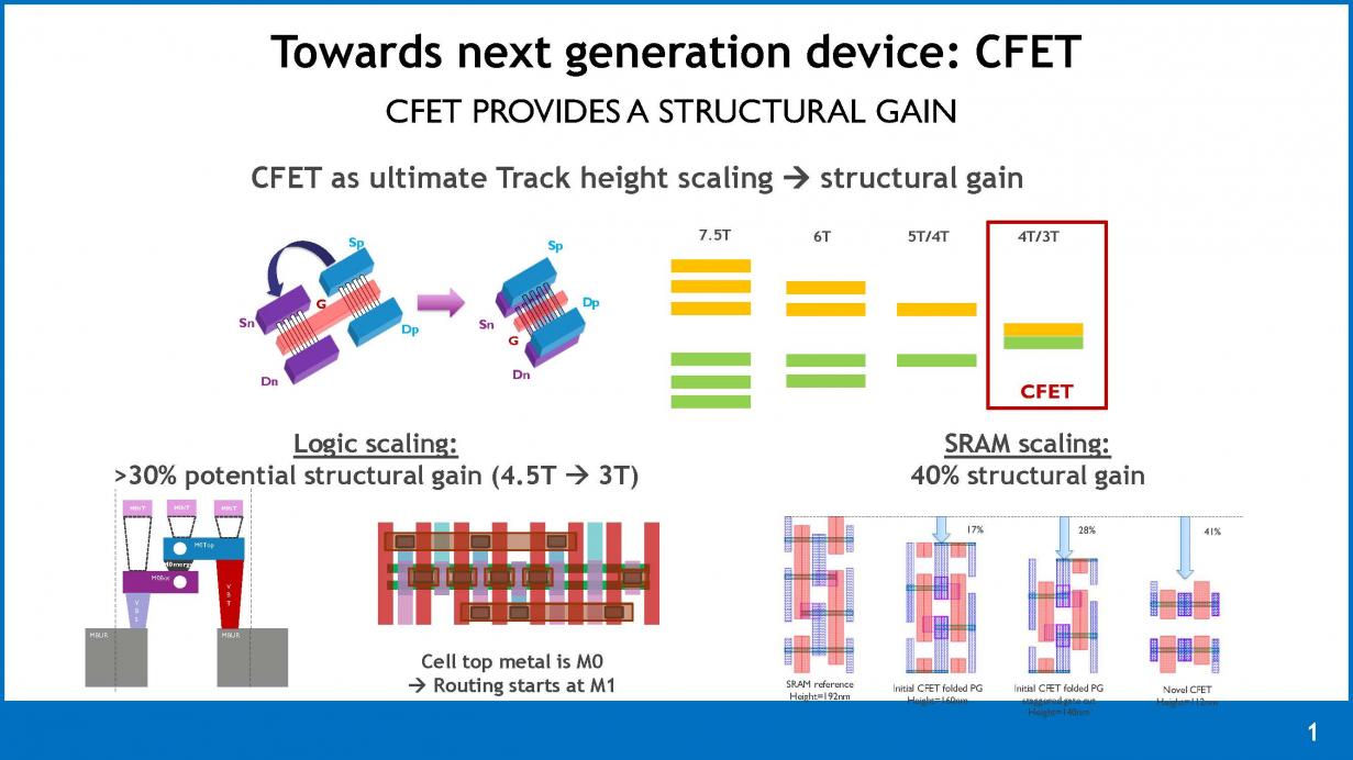
The 2018 VLSI Technology conference was held in Hawaii in June and is one of the premier conferences covering integrated circuit process technology and circuit design. The Complementary FET (CFET) is an emerging option to continue logic scaling into the next decade. At the conference imec, GLOBALFOUNDRIES, Tokyo Electron and… Read More
There has been a lot of new information available about the leading-edge logic processes lately. Papers from IEDM in December 2017, VLSIT this month, the TSMC and Samsung Foundry forums, etc. have all filled in a lot of information. In this article I will summarize what is currently known.… Read More
At IEDM in December I had a chance to interview Thomas Ernst about the paper “Performance and Design Considerations for Gate-All-around Stacked-NanoWires FETs” by Leti and STMicroelectonics.
Leti published the first stacked nanowire in 2006, it was very new then, now stacked nanowire/nanosheets are starting… Read More
At the IEDM 2017, imec held an imec technology forum and presented several papers, I also had the opportunity to interview Anda Mocuta director of technology solutions and enablement. In this article I will summarize the keys points of what I learned about the future of logic. I will follow this up with a later article covering memory.… Read More


