You are currently viewing SemiWiki as a guest which gives you limited access to the site. To view blog comments and experience other SemiWiki features you must be a registered member. Registration is fast, simple, and absolutely free so please,
join our community today!
Last month Cadenceannounced its fastest parasitic extraction tool (minimum 5 times better performance compared to other available tools) which can handle growing design sizes with interconnect explosion, number of parasitics and complexities at advanced process nodes including FinFETs, without impacting accuracy of … Read More
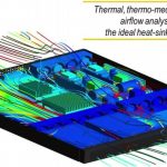
Last week my daughter was playing some games on my Google Nexus smartphone for a while when one of my friends called. When I picked up the phone, I couldn’t imagine it was so hot. There is no doubt; every electronic device today emits an order of magnitude higher heat than what it used to at most a decade ago. There is so much emphasis on … Read More
In my career in semiconductor industry, I can recall, in the beginning there was emphasis on design completion with automation as fast as possible. The primary considerations were area and speed of completion of a semiconductor design. Today, with unprecedented increase in multiple functions on the same chip and density of the… Read More
Last night the IEEE Silicon Valley Chapter had a panel session that was in some ways a preview of some of what will be discussed at the Electronic Design Process Symposium in Monterey next Thursday and Friday. At EDPS Herb Reiter organized a session on FinFET, 3DIC and FD-SOI (sort of how many buzzwords can you get into one set of titles).… Read More
AMD Goes 3Dby Paul McLellan on 12-13-2013 at 7:16 pmCategories: EDA
I attended the 3D packaging conference in Burlingame this week. The most interesting presentation to me was by Bryan Black of AMD. He argued very convincingly that Moore’s Law is basically over for the PC microprocessor business and the way forward is going to be 3D. AMD are clearly working on all this.
Increased density and… Read More
Two conferences on 3D, one just over and one coming up next week. The one that was just over was hosted by Georgia Tech, the 3rd Annual Global Interposer Technology Workshop (GIT). I wasn’t there but my ex-colleague from VLSI Technology Herb Reiter was. Herb has become very much associated with all things 3D since he led the … Read More
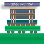
For the tenth year, the big 3DIC conference takes place in the Hyatt Regency at Burlingame (just south of San Francisco Airport). Officially it is 3D Architectures for Semiconductor Integration and Packaging or ASIP. This year there have already been some significant 3D announcements: TSMC’s 3D program, and Micron’s… Read More
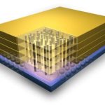
Today Micron announced that it is shipping 2GB Hybrid Memory Cube (HMC) samples. The HMC is actually 5 stacked die connected with through-silicon-vias (TSVs). The bottom die is a logic chip and is actually manufactured for Micron in an IBM 32nm process (and doesn’t have any TSVs). The other 4 die are 4Gb DRAM die manufactured… Read More
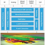
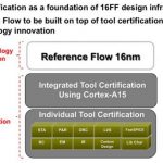
Today TSMC announced three reference flows that they have been working on along with various EDA vendors (and ARM and perhaps other IP suppliers). The three new flows are:
- 16FinFET Digital Reference Flow. Obviously this has full support for non-planar FinFET transistors including extraction, quantized pitch placement, low-vdd
…
Read More
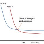
With the uncertainties around timing of 450mm wafers, EUV (whether it works at all and when) and new transistor architectures it is unclear whether Moore’s law as we know it is going to continue, and in particular whether the cost per transistor is going to remain economically attractive especially for consumer markets … Read More