You are currently viewing SemiWiki as a guest which gives you limited access to the site. To view blog comments and experience other SemiWiki features you must be a registered member. Registration is fast, simple, and absolutely free so please,
join our community today!
Now that the dust has settled let’s talk more about TSMC’s Open Innovation Platform. Launched in 2008, OIP represents a groundbreaking collaborative model in the semiconductor industry. Unlike IDMs that controlled the entire supply chain, OIP fosters an “open horizontal” ecosystem uniting TSMC… Read More
Todd Burkholder and Andras Vass-Varnai, Siemens EDA
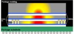
As semiconductor devices become smaller, more powerful and more densely integrated, thermal management has shifted from an afterthought to a central challenge in modern IC design. In contemporary 3D IC architectures—where multiple chiplets are stacked and closely arrayed—power… Read More
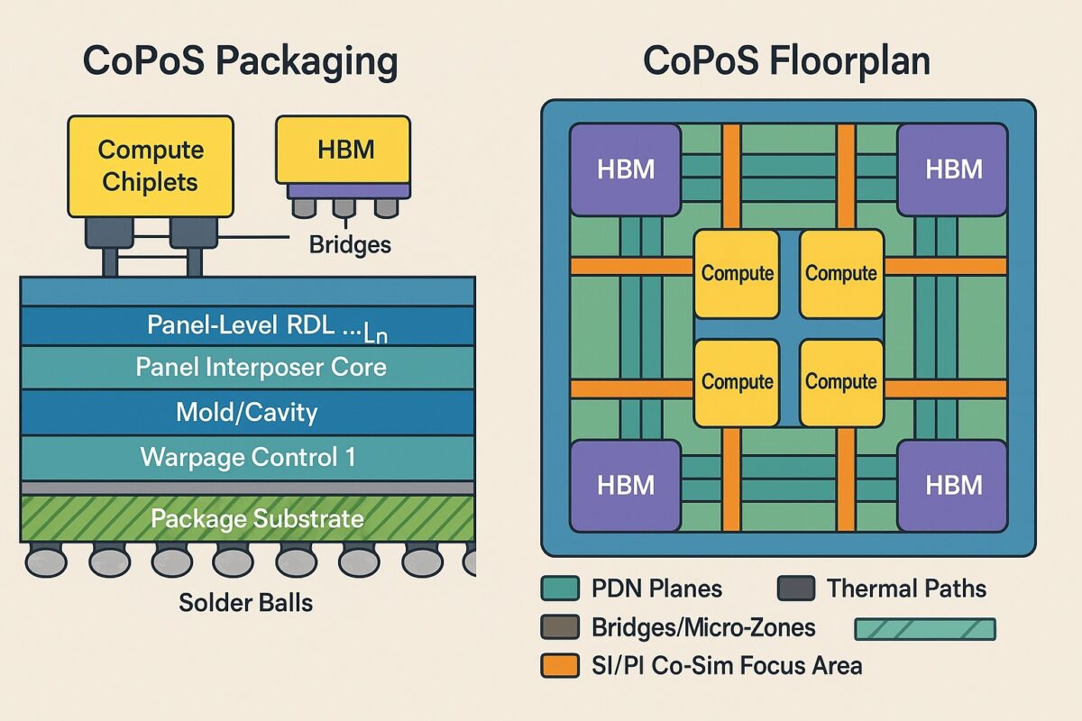
Chip on Panel on Substrate, often shortened to CoPoS, extends the familiar idea of chip on carrier packaging by moving the redistribution and interposer style structures from circular wafers to large rectangular panels. The finished panel assembly is then mounted on an organic or glass package substrate. This shift from round
…
Read More
Bob Fung is the CEO of Owens Design, a Silicon Valley company specializing in the design and build of complex equipment that powers high-tech manufacturing. Over his 22-year tenure, Bob has led the development of more than 200 custom systems for world-class companies across the semiconductor, biomedical, energy, and emerging… Read More
The demand for higher performance, greater configurability, and more cost-effective solutions is pushing the industry toward heterogeneous integration and 3D integrated circuits (3D ICs). These solutions are no longer reserved for niche applications—they are rapidly becoming essential to mainstream semiconductor design.… Read More
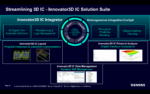
The semiconductor industry is rapidly moving beyond traditional 2D packaging, embracing technologies such as 3D integrated circuits (3D ICs) and 2.5D advanced packaging. These approaches combine heterogeneous chiplets, silicon interposers, and complex multi-layer routing to achieve higher performance and integration.… Read More
In a major announcement at the 2025 Design Automation Conference (DAC), Siemens EDA introduced a significant expansion to its electronic design automation (EDA) portfolio, aimed at transforming how engineers design, validate, and manage the complexity of next-generation three-dimensional integrated circuits (3D ICs).… Read More
In a keynote delivered at this year’s Siemens EDA User2User event, CEO Mike Ellow presented a focused vision for the evolving role of electronic design automation (EDA) within the broader context of global technology shifts. The session covered Siemens EDA’s current trajectory, market strategy, and the changing landscape … Read More
In this episode of the Semiconductor Insiders video series, Dan is joined by Anna Fontanelli, founder and CEO of MZ Technologies. Anna explains some of the substantial challenges associated with heterogeneous 3D integration. Dan then begins to explore some of the capabilities of GenioEVO, the first integrated chiplet/package… Read More