While this was not specifically stated, it was certainly implied during the sessions I attended at SEMICON West this week: The traditional semiconductor business model (IDM) is coming to an end. Starting with the keynote: Foundry-driven Innovation in the Mobility Era,cost was the common theme in any discussion involving mobile… Read More
Tag: 20nm
Avoiding layout related variability issues
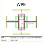
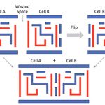
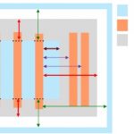
In advanced process technologies, electrical and timing problems due to variability can become a big issue. Due to various processing effects, a circuit performance (both speed and power) is dependent on specific layout attributes and can vary a lot from instance to instance. The accumulated effects can be severe to the point… Read More
How To Design a TSMC 20nm Chip with Cadence Tools
Every process node these days has a new “gotcha” that designers need to be aware of. In some ways this has always been the case but the changes used to be gradual. But now each process node has something discontinuously different. At 20nm the big change is double patterning. At 14/16nm it is FinFET.
Rahul Deokar and John… Read More
Challenges of 20nm IC Design
Designing at the 20nm node is harder than at 28nm, mostly because of the lithography and process variability challenges that in turn require changes to EDA tools and mask making. The attraction of 20nm design is realizing SoCs with 20 billion transistors. Saleem Haider from Synopsys spoke with me last week to review how Synopsys… Read More
TSMC ♥ Solido
Process variation has been a top trending term since SemiWiki began as a result of the articles, wikis, and white papers posted on the Solido landing page. Last year Solido and TSMC did a webinar together, an article in EETimes, and Solido released a book on the subject. Process variation is a challenge today at 28nm and it gets worse… Read More
Moore, or More Than Moore?
Yesterday was the 2013 GSA Silicon Summit, which was largely focused on contrasting what advances in delivering systems will depend on marching down the ladder of process nodes, and which will depend on innovations in packaging technology. So essentially contrasting Moore’s Law with what has come to be known as More Than… Read More
Two New TSMC-Cadence Webinars for Advanced Node Design
Foundries and EDA vendors are cooperating at increasing levels of technical intimacy as we head to the 20nm and lower nodes. Cadence has a strong position in the EDA tools used for IC design and layout of custom and AMS (Analog Mixed-Signal) designs. They have created a series of webinars to highlight the design challenges and new… Read More
TSMC Responds to Samsung!
This was the 19[SUP]th[/SUP] annual TSMC Symposium and by far the best I have attended. Finally tired of the misinformation that plagues our industry, TSMC set the record straight with wafer and silicon correlated data. TSMC shipped more than 88 MILLION logic wafers in 2012, more than any other semiconductor company, that gives… Read More
TSMC on Collaboration: JIT Ecosystem Development
Cliff Hou of TSMC gave the keynote today at SNUG on Collaborate to Innovate: a Foundry’s Perspective. Starting around 45nm the way that a foundry has to work with its ecosystem fundamentally changed. Up until then, each process generation was similar enough to the previous one, apart obviously from size, that it could be … Read More
Reliability is the New Power
It has be come a cliche to say that “power is the new timing”, the thing that keeps designers up at night and drives the major architectural decisions in big SoCs. Nobody is saying it yet but perhaps “reliability is the new power” will be tomorrow’s received wisdom.
I talked to Adrian Evans of IROCTech… Read More


