You are currently viewing SemiWiki as a guest which gives you limited access to the site. To view blog comments and experience other SemiWiki features you must be a registered member. Registration is fast, simple, and absolutely free so please,
join our community today!
Synopsys ♥ FinFETsby Daniel Nenni on 03-03-2013 at 6:00 pmCategories: EDA, Synopsys
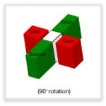
FinFETs are fun! They certainly have kept me busy writing over the past year about the possibilities and probabilities of a disruptive technology that will dramatically change the semiconductor ecosystem. Now that 14nm silicon is making the rounds I will be able to start writing about the realities of FinFETs which is very exciting!… Read More
Tech aficionados love roadmaps. The confidence a roadmap instills – whether using tangible evidence or just a good story – can be priceless. Decisions on “the next big thing”, sometimes years and a lot of uncertain advancements away, hinge on the ability of a technology marketing team to define and communicate a roadmap.
Any roadmap… Read More
The industry plans to use 193nm light at the 20nm, 14nm, and 10nm nodes. Amazing, no? There is no magic wand; scientists have been hard at work developing computational lithography techniques that can pull one more rabbit out of the optical lithography hat.
Tortured metaphors aside, the goal for the post-tapeout flow is the same… Read More
I was at the Common Platform Technology Forum this week. One of the most interesting sessions is IBM’s Gary Patton giving an overview of the state of semiconductor fabrication. Then, at lunchtime, he is one of the people that the press can question. In this post, I’m going to focus on Extreme Ultra-Violet (EUV) lithography.… Read More
Can’t make it to Santa Clara? Join us online!
The detailed 2013 CPTF agenda is now up in preparation for the February 5th event at the Santa Clara Convention Center. This is one of the rare times that you can get a free lunch! Watch this quick video to see what is in store for us this year. Dr. Paul McLellan and I will be there so please… Read More
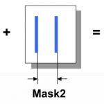
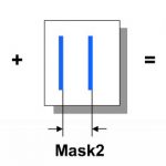
TSMC and Synopsys hosted a webinar in December on this topic of double patterning and how it impacts the IC extraction flow. The 20nm process node has IC layout geometries so closely spaced that the traditional optical-based lithography cannot be used, instead lower layers like Poly and Metal 1 require a new approach of using two… Read More
We know by now that clock speeds aren’t everything when it comes to measuring the goodness of a processor. Performance has direct ties to pipeline and interconnect details, power factors into considerations of usability, and the unspoken terms of yield drive cost.
My curiosity kicked in when I looked at the recent press release… Read More
You can’t have failed to notice that 20nm is coming. There are a huge number of things that are different about 20nm from 28nm, but far and away the biggest is the need for double patterning. You probably know what this is by now, but just in case, here is a quick summary.
Lithography is done using 193nm light. Today we use immersion… Read More
Tim Cook’s strategy to disengage from Samsung as a supplier of LCDs, memory and processors while simultaneously creating a worldwide supply chain from the remnants of former leaders like Sharp, Elpida, Toshiba and soon Intel is remarkable in its scope and breadth. By 2014, Apple should have in place a supply chain for 500M iOS devices… Read More
Solido Design Automation and TSMC recently published an article in EE Times describing how Solido’s High-Sigma Monte Carlo tool is used with TSMC PDK’s to achieve high-yield, high-performance memory design. This project has been a big part of my life for the past three years and it is time for a victory lap!
In TSMC 28nm, 20nm and … Read More