Seeking Alpha just published an article about Intel and Samsung passing TSMC for process leadership. The Intel part seems to be a theme with them, they have talked in the past about how Intel does bigger density improvements with each generation than the foundries but forget that the foundries are doing 5 nodes in the time it takes… Read More
Tag: 10nm
Leading Edge Foundry Wafer Prices
I have seen several articles recently discussing foundry wafer selling prices for leading edge wafers, these articles all quote estimates from a paper by the Center for Security and Emerging Technology (CSET). The paper is available here.
My company IC Knowledge LLC is the world leader in cost and price modeling of semiconductors… Read More
Fully Self-Aligned 6-Track and 7-Track Cell Process Integration
For the 10nm – 5nm nodes, the leading-edge foundries are designing cells which utilize 6 or 7 metal tracks, entailing a wide metal line for every 4 or 5 minimum width lines, respectively (Figure 1).
Figure 1. Left: a 7-track cell. Right: a 6-track cell.
This is a fundamental vulnerability for lithography, as defocus can change… Read More
A “Super” Technology Mid-life Kicker for Intel
Summary
At the recent Intel Architecture Day 2020 symposium, a number of technology enhancements to the Intel 10nm process node were introduced. The cumulative effect of these enhancements would provide designs with a performance boost (at iso-power) approaching 20% – a significant intra-node enhancement, to be sure. The… Read More
Effect of Design on Transistor Density
I have written a lot of articles looking at leading edge processes and comparing the process density. One comment I often get are that the process density numbers I present do not correlate with the actual transistor density on released products. A lot of people want to draw conclusions an Intel’s processes versus TSMC’s processes… Read More
LithoVision – Economics in the 3D Era
Each year on the Sunday before the SPIE Advanced Lithography Conference, Nikon holds their LithoVision event. This year I had the privilege of being invited to speak for the third consecutive year, unfortunately, the event had to be canceled due to concerns over the COVID-19 virus but by the time the event was canceled I had already… Read More
LithoVision 2019 – Semiconductor Technology Trends and their impact on Lithography
I was asked to present at Nikon’s LithoVision event again this year. LithoVision is held the day before the SPIE Advanced Lithography Conference also in San Jose. The following is a write up of my talk.… Read More
IEDM 2018 Imec on Interconnect Metals Beyond Copper
At IEDM this December Imec presented “Interconnect metals beyond copper – reliability challenges and opportunities”. In addition to seeing the paper presented I had a chance to interview one of the authors, Kristof Croes. Replacements for copper are a hot subject and I will summarize the challenges and Imec’s work.… Read More
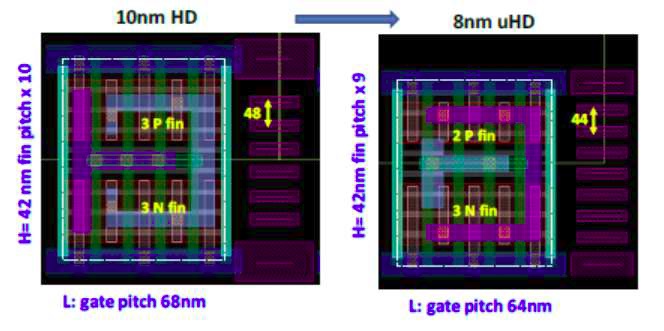
Samsung 10nm 8nm and 7nm at VLSIT
I got a tip sheet today for the upcoming 2018 Symposia on VLSI Technology & Circuits to be held June 19th through 21st in Honolulu, Hawaii. There is some interesting information on Samsung’s 10nm, 8nm and 7nm processes in the tip sheet:… Read More
Intel 10nm Yield Issues
On their first quarter earnings call Intel announced that volume production of 10nm has been moved from the second half of 2018 to 2019 due to yield issues. Specifically, they are shipping 10nm in low volume now, but yield improvement has been slower than anticipated. They report that they understand the yield issues but that improvements… Read More


