TSMC has established a leadership position among silicon foundries, based on three foundational principles:
- breadth of technology support
- innovation in technology development
- collaboration with customers
Frequent SemiWiki readers have seen how these concepts have been applied to the fabrication and packaging technology roadmaps, which continue to advance at an amazing cadence. Yet, sparse coverage has typically been given to TSMC’s focus on process and customer product reliability assessments – these principles are also fundamental to the reliability ecosystem at TSMC.
At the recent International Reliability Physics Symposium (IRPS 2022), Dr. Jun He, Vice-President of Corporate Quality and Reliability at TSMC, gave a compelling keynote presentation entitled: “New Reliability Ecosystem: Maximizing Technology Value to Serve Diverse Markets”. This article provides some of the highlights of his talk, including his emphasis on these principles.
Technology Offerings and Reliability Evaluation
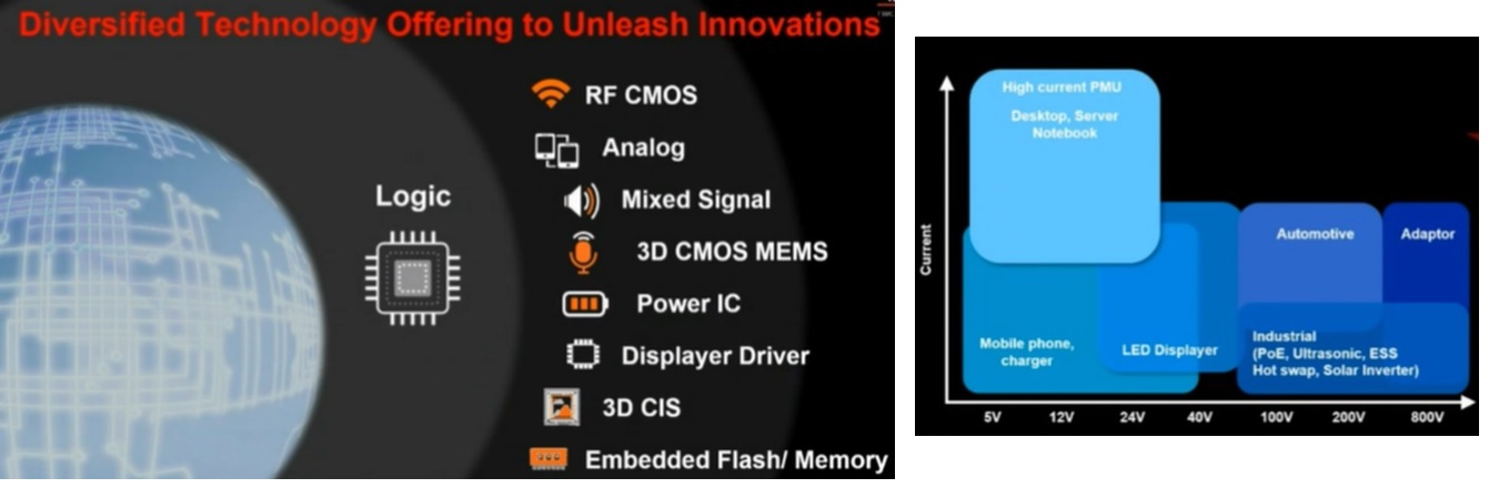
The figures above highlight the diverse set of technologies that Dr. He’s reliability team needs to address. The reliability stress test methods for these technologies vary greatly, from the operating voltage environment to unique electromechanical structures.
Dr. He indicated, “Technology qualification procedures need to be tailored toward the application. Specifically, the evaluation of MEMS technologies necessitates unique approaches. Consider the case of an ultrasound detector, where in its end use the detector is immersed in a unique medium. Our reliability evaluation methods need to reflect that application environment.”
For more traditional microelectronic technologies, the reliability assessments focus on accelerating defect mechanisms, for both devices and interconnect:
- hot carrier injection (HCI)
- bias temperature instability (NBTI for pFETs, PBTI for nFETs)
- time-dependent dielectric breakdown (TDDB)
- electromigration (for interconnects and vias)
Note that these mechanisms are highly temperature-dependent.
As our understanding of the physics behind these mechanisms has improved, the approaches toward evaluating their impact to product application failure rates have also evolved.
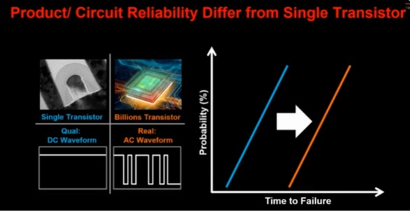
Dr. He commented, “Existing JEDEC stress test standards are often based on mechanism acceleration using a DC Vmax voltage. However, customer-based product qualification feedback did not align with our technology qualification data. Typically, the technology-imposed operating environment restrictions were more conservative.”
This is of specific interest to high-performance computing (HPC) applications, seeking to employ boost operating modes at increased supply voltages (within thermal limits).
Dr. He continued, “We are adapting our qualification procedures to encompass a broader set of parameters. We are incorporating AC tests, combining Vmax, frequency, and duty cycle variables.”
The nature of “AC recovery” in the NBTI/PBTI mechanism for device Vt shift has been recognized for some time, and is reflected in device aging models. Dr. He added, “We are seeing similar recovery behavior for the TDDB defect mechanism. We are aggressively pursuing reliability evaluation methods and models for AC TDDB, as well.”

The figure above illustrates the how the Vt shift due to BTI is a function of the duty cycle for the device input environment, as represented by the ratio of the AC-to-DC Vt difference. The figure also highlights the newer introduction of a TDDB lifetime assessment for high-K gate dielectrics, as a function of input frequency and duty cycle.
Parenthetically, Dr. He acknowledged that end application product utilization can vary widely, and that AC reliability testing makes some usage assumptions. He indicated that TSMC works with customer to establish appropriate margins for their operating environment.
Reliability Evaluation of New Device Types
TSMC has recently added resistive RAM (RRAM) and magneto-resistive RAM (MRAM) IP to their technology offerings.
The unique physical nature of the resistance change in the storage device for these technologies necessitates development of a corresponding reliability evaluation procedure, to establish retention and endurance specifications. (For the MRAM technology, the external magnetic field immunity specification is also critical.)
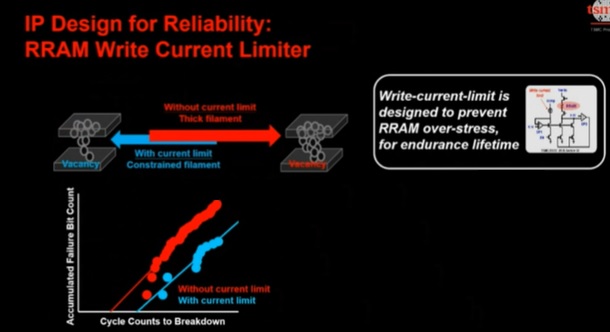
For both these technologies, the magnitude and duration of the write current to the storage cell is a key design parameter. The maximum write current is a crucial reliability factor. For the MRAM example, a high write current through the magnetic tunnel junction to set/reset the orientation of the free magnetic layer in the storage cell degrades the tunnel barrier.
TSMC collaborates with customers to integrate write current limiting circuits within their designs to address the concern. The figure below illustrates the write current limiter for the RRAM IP.
TSMC and Customer Collaboration Reliability Ecosystem
In addition to the RRAM and MRAM max write current design considerations, Dr. He shared other examples of customer collaborations, which is a key element of the reliability ecosystem.
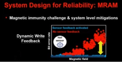
Dr. He. shared the results of design discussions with customers to address magnetic immunity factors – the figure below illustrates cases where the design integrated a Hall effect sensor to measure the local magnetic field. The feedback from the sensor can be used to trigger corrective actions in the write cycle.
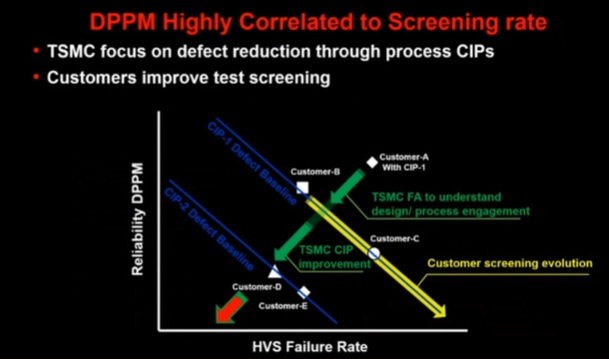
The customer collaboration activities also extend beyond design for reliability (DFR) recommendations. TSMC shares defect pareto data with customers. Correspondingly, the TSMC DFR and design-for-testability (DFT) teams will partner with customers to incorporate key defect-oriented test screens into the production test flow.
Dr. He provided the example where block-specific test screens may be appropriate, as illustrated below.
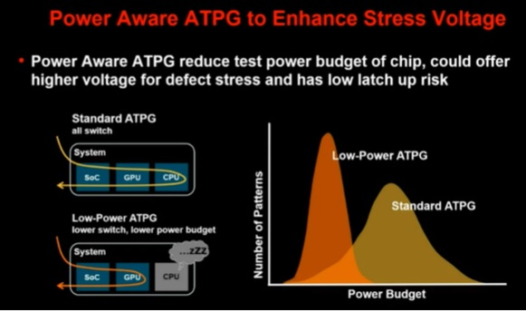
Power management design approaches may be needed across the rest of the design to accommodate block-level test screens.
The figure below depicts the collaboration model, showing how customer reliability feedback is incorporated into both the test environment and as a driver for continuous improvement process (CIP) development to enhance the technology reliability.
Summary
At the recent IRPS, TSMC presented their reliability ecosystem, encompassing:
- developing unique reliability programs across a wide breadth of technologies (e.g., MEMS)
- developing new reliability methods for emerging technologies (e.g., RRAM, MRAM)
- sharing design recommendations with customers to enhance final product reliability
- collaborating closely with customers on DFR issues, and integrating customer feedback into DFT screening procedures and continuous improvement process focus
Reflecting upon Dr. He’s presentation, it is no surprise that these reliability ecosystem initiatives are consistent with TSMC’s overall principles.
-chipguy
Also read:
Self-Aligned Via Process Development for Beyond the 3nm Node
Technology Design Co-Optimization for STT-MRAM
Advanced 2.5D/3D Packaging Roadmap
Share this post via:


Comments
There are no comments yet.
You must register or log in to view/post comments.