EDA companies and foundries must closely collaborate in order to deliver IC tool flows that work without surprises at the 40nm and 28nm nodes.
Tomorrow in San Jose you can attend this 4th annual event hosted by TSMC along with Mentor Graphics and other EDA and IP companies.
Here are some of the topics that will interest IC designers using Mentor tools:
iLVS: Accessible, Supportable Paradigm for Circuit Verification at Advanced Nodes (2:30PM, EDA Track)
Accurate, comprehensive device recognition, connectivity extraction, netlist generation and, ultimately, circuit comparison becomes more complex with each new process generation. The number of layers and layer derivations are increasing and the complexity of devices, especially Layout Dependent Effects (LDS), becomes harder and harder to model. In the past, customers could take a foundry rule deck and easily modify it to include their own device models for transistors, resistor, capacitors, inductors, etc., and even augment the deck with their own checks. At 40nm, 28nm, few customers are able to do this confidently. To address this situation, TSMC and Mentor Graphics will discuss how they collaborated to define iLVS, a syntax that provides customers with a more easily adaptable solution to their circuit verification needs. Using iLVS, users can more easily modify and augment foundry rule decks, yet still adhere to the modeling and manufacturing intent captured in these decks.
Keys to Successful DFM Partnership (4:00PM,IP/EDA/Services Track)
DFM is now a known necessity for advanced nodes. But a successful DFM strategy is more than a “push button” solution. It depends on a synergistic combination of tool technology and design methodology, and close collaboration with the foundry. In this session, CSR and Mentor will relate their personal experiences with DFM, its implementation in the TSMC ecosystem, discuss critical factors that determine the difference between success and failure in actual practice.
Challenges and Directions for Next Generation 3D-IC (4:30PM, EDA Track)
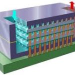
The IC industry is steadily moving to the third dimension of scaling, i.e., stacking die vertically using through silicon vias (TSVs) to make inter-die connections in a manner analogous to copper vias in multi-layer printed circuit boards (PCBs), but on a much smaller scale. The 2.5D interposer solution is here today, but next generation, ergo full 3D, will bring additional complexities. For example, when TSVs are introduced into the active area of an IC, things get complicated due to complex electrical, mechanical stress and thermal interactions that impact circuit performance and reliability. In this session Qualcomm and Mentor Graphics will discuss some of the challenges of designing 3D-ICs and what the ecosystem is doing to provide the needed methods and tools to make next generation 3D-IC a reality.
Improving Analog/Mixed Signal Circuit Reliability at Advanced Nodes (5:00PM,IP/EDA/Services Track)
Preventing electrical circuit failure is a growing concern for IC designers today. For certain types of failures such as Electrostatic discharge (ESD) issues, there are well established best practices and design rules that circuit designers should be adhering to. Other issues are more recent, such as the best way to design circuits that cross different voltage regions on a chip. While these topics are not unique to a specific technology node, in particular for analog mixed signal they become increasingly critical as the oxides get thinner for the most advanced nodes and as circuit designers continue to put more and more voltage regions on-chip. To validate that circuits have robust protection from electrical failure, TSMC and MGC will present how they have partnered to define and develop rule decks that enable automatic advanced circuit verification to address these issues at the 28nm and 40nm nodes.
Information on the TSMC Open Innovation Platform Ecosystem Forum is here.