Talking about Design IP (I mean successful Design IP) lead you to quickly pronounce the two magic key words: Quality and Ecosystem. Those who remember the IP emergence in the mid 90’s know very well why Quality has to be a prerequisite when dealing with Design IP, as they probably have paid the price of mediocre IP quality at that time. More recently, business analysts have realized that the foundation for a successful IP based business was linked to building a complete Ecosystem, just think about the 1000 ARM partners…
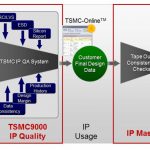
As a matter of fact, some of these partners are heavyweight, like Taiwan based TSMC, that any IP vendor would like to count within it IP Ecosystem. That’s why TSMC has created, back in 2000, the TSMC9000 program as one of the pillar of Open Integration Platform (OIP) ecosystem. TSMC9000 clearly defined goal is to check for, assess and audit the quality of Design IP part of OIP ecosystem. TSMC9000 is not only based on cleaver communication, but on a very rigorous process! Don’t forget that any of this Design IP function will end up into a very concrete piece of Silicon, an Integrated Circuit, and that both TSMC (who process it into Wafer Fab) and the Fabless customer who plan to sell it, expect this IC to run first time right. As an IP vendor, you submit to TSMC (in fact to “IP Portfolio, Design Infrastructure Division”) the functional IP you have developed, from USB PHY to DDR Memory Controller, LVDS I/O to DSP and many more. TSMC9000 Quality Assurance system consists to run successively:
- DRC/LVS (if you submit Hard IP)
- Data Consistency check
- ESD tolerance verification
- Design margin verification (Shmoo plot)
- Then generate Silicon reports (on Test chips) and store production history when it’s relevant.
Your IP will hopefully be sold to customer, integrated into a design data base by this customer who will finally submit the final DB for Tape Out. At this stage, TSMC will use “IP Master” tool, running “Tape Out consistency checks” versus the previously generated data in IP9000 IP Quality.
You may wonder that TSMC9000 IP qualification process only applies to very complexes or very specific or “exotic” Design IP… In fact, if you take a look at the above picture, you realize that TSMC9000 apply to ALL the Libraries, Memories or IP, including Hard and Soft IP. How many IP would you guess? Are we talking about 500 Design IP, or 1000, maybe 2000? Just take a look at the statistics listed below…
There are no less than 8917 active IP coming from the IP Alliance for a total of almost 10, 000 IP in TSMC 9000! Another figure is surprising: almost 200 Design IP are being reviewed every month by TSMC. This means that TSMC has built a specific team 100% dedicated to run IP9000 QA Process, a 30 people team in charge of IP Port-Folio validation (and selection). As an IP vendor, you probably better understand why TSMC has to be highly selective when accepting new IP… Are you still in IP vendor shoes? Just look at the failed TSMC 9000 IP count: 1,452!!
Even if a dummy density violation or some Silicon corner out of specification can be accounted for a failure, out of these 1,452 IP, as high as 373 can generate potential fatal failure. Fatal simply means that a Tape Out including such IP would have led to a redesign. Thus, if you go now into Fabless shoes, you will just thank your foundry supplier for being so selective!
If you ever surfed on a foundry web site, you probably remember the “Bronze”, “Silver” and “Gold” denomination for Design IP. If you look at the above picture, these denominations look a little bit obsolete: before a Design Hard IP can be validated for volume production, it has to pass through no less than ten or more verification phases, before the Design IP can reach a high enough confidence level. If we consider advanced nodes, the Hard IP has to pass through 13 various checking phases, from DRC, LVS, ERC and Antenna checks up to Split Lot Silicon Assessment, testing results audits by TSMC test lab to finally go to production. In fact, Quality assessment is a never ending process, when the ASIC or ASSP is in volume production, the IC yield is continuously traced… probably up to the product End Of Life!
I didn’t know that Quality could be a fascinating topic (to be honest, I thought it was not), but we are working in such demanding industry that even Quality becomes part of the dream: I have today in my pocket a gaming station from the 2000’s, a phone from the 90’s, a color TV from the 80’s and a Supercomputer from the 70’s, all of these almost in a single chip!
Eric Esteve
lang: en_US