
Soitec is a unique company that is at the center of major changes in our industry. Technology megatrends are fueling massive demand for semiconductors and this has increased the adoption of engineered substrates. As a global leader in the development of engineered substrates, Soitec is a company to watch. While this technology finds use across many areas of semiconductor application, photonics is a particularly important area that is enabled by Soitec and its engineered substrates. The company recently published a very informative white paper on the topic. A link is coming so you can get your own copy. First, let’s explore a bit about the company and its strategy to see how Soitec delivers the foundation for next-generation interconnects.
About Soitec
With the demands of density, performance and power efficiency required for advanced semiconductors, it turns out that silicon in its purest form often falls short to deliver on all the requirements. Adding additional materials to the silicon can enhance its capabilities, but adding an epitaxial layer of new material to silicon can be both difficult and unpredictable. Soitec has developed a process to deliver engineered substrates that addresses these challenges, opening new opportunities for innovation. You can learn about some of the things Soitec is doing here.
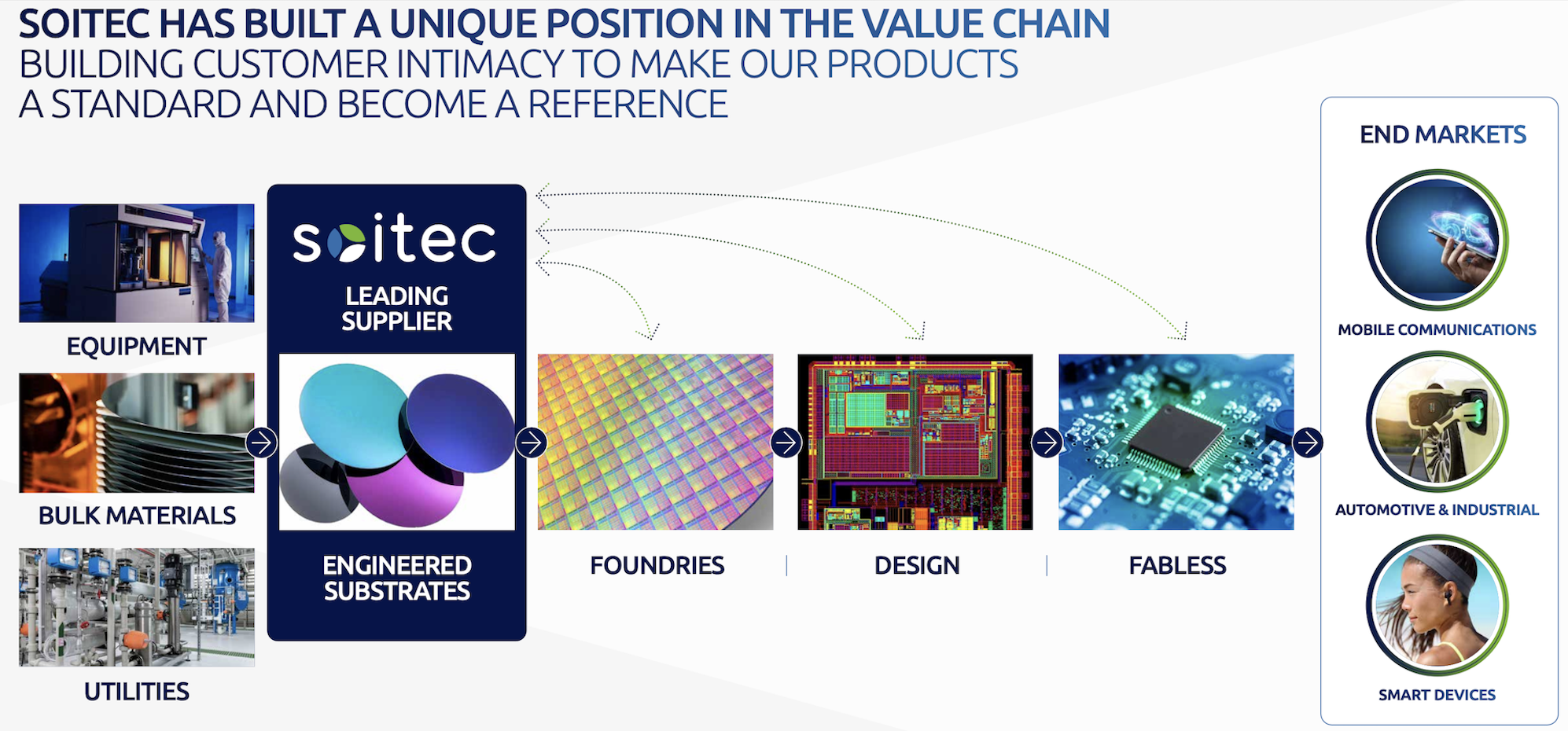
Thanks to the increasing adoption of engineered substrates, the company expects its addressable market to grow by 3X between 2022 and 2030. The breadth of Soitec’s impact is illustrated in the figure below.
About Photonics
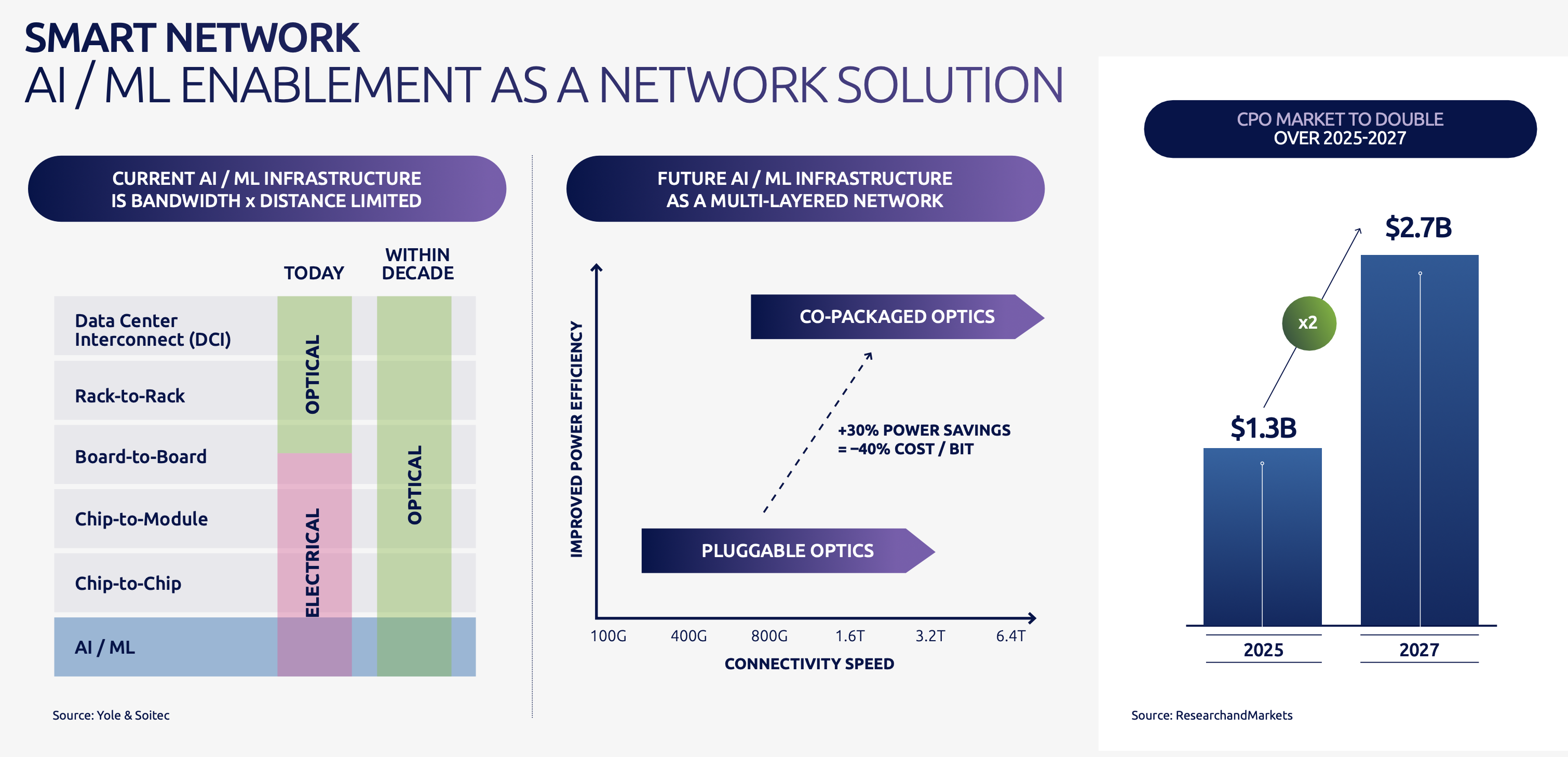
As with many trends, AI/ML is a main driver for photonics adoption. The current infrastructure for these applications is bandwidth and distance limited. A move to optical interconnect is on the horizon that will open new possibilities. The figure below summarizes these trends.
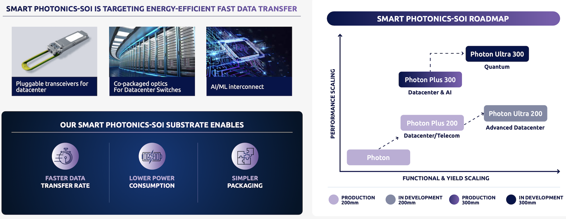
To address these opportunities, Soitec has a roadmap that is summarized below.
With this backdrop, I’ll provide a summary of the new white paper.
About the White Paper
The new white paper is appropriately titled, Has Silicon Photonics Finally Found It’s Killer Application? The piece explains how engineered silicon substrates are providing the foundation for the cutting-edge photonics engines that data centers will need to usher in the era of artificial intelligence.
The piece talks about the onset of artificial intelligence and machine learning that leverage large language models (LLMs) for both AI training and inference. These models exhibit a super-exponential growth in modeling parameters. As a result, inter-data and especially intra-data center traffic has exploded, requiring the need for high-speed optical pluggable transceivers. These devices are currently transitioning from 100 Gbps to 400 Gbps. Some shipments of 800-Gbps devices already started in 2023 and even 1.6-Tbps pluggables are also available today for pre-sampling.
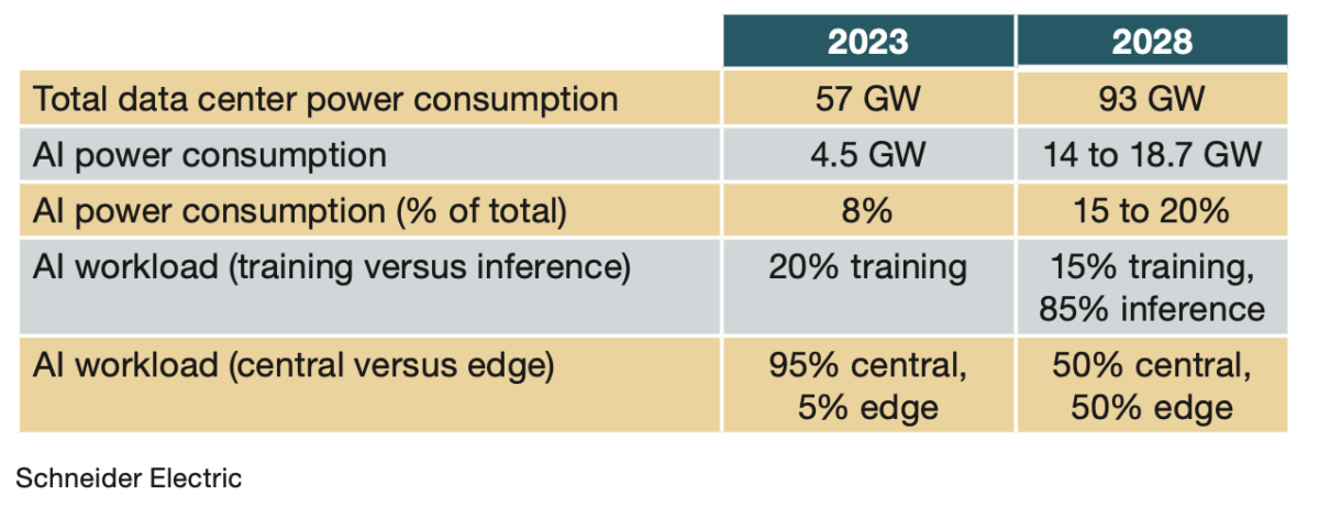
The piece goes on to explain that optical transceivers must address three different key requirements: high speed, low power, and minimized cost. Regarding power, server clusters in a data center deliver power densities between 50 and 100 kW to meet new AI requirements. However, the share of AI workloads in a data center is expected to more than double between 2023 and 2028. How these trends impact power consumption is illustrated in the table below.
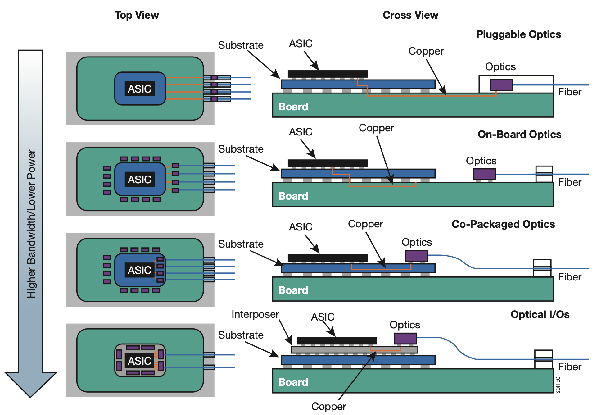
This means there is a significant need for lower-power, higher-speed optical transceivers as data volume grows, which is driving pluggable form factors to evolve. The piece points out that the digital signal processing (DSP) chip inside pluggable transceivers is one of the main sources of power consumption. This has led to exploration of novel transceiver designs, such as linear-drive pluggable optics (LPOs), half-retimed linear optics (HALOs), and co-packaged optics (CPOs), that use advanced device design and photonics-electronics co-integration. This would enable future pluggables to operate in direct-drive, without a stand-alone, dedicated DSP component.
The figure below illustrates this evolution.
The white paper then discusses the changes on the horizon to optimize power, performance and cost of AI architectures, with a focus on transceiver design. As shown earlier, silicon photonics will play a major role in these changes. And silicon-on-insulator technology has unique properties to address the demanding requirements of silicon photonics.
The details of Soitec’s engineered substrates to address these requirements is presented in detail. There is a lot of great information presented – you should get a copy of this white paper. A link is coming.
The Executive Viewpoint

René Jonker has recently been named as the SVP & GM of Smart Devices Division at Soitec. He oversees Imager, FD-SOI for IoT applications and silicon photonics. I had the opportunity to speak with René recently to get his view of the trends regarding silicon photonics and Soitec’s position in this growing market.
René began by discussing the mega-trends that are creating the disruption we are currently seeing. He cited the growth in size and scale of data centers and the associated increased demand for bandwidth as important drivers. He also mentioned the power consumption that comes along with these changes; this was a big topic at the recent OFC Conference in San Francisco.
He commented that electrical interconnects will still have a place – primarily in server backplanes where the technology can deliver cost-effective performance. From a system perspective, he felt that photonics and optical interconnects are really the only technology to address the previously mentioned demands and manage power consumption at the same time. René mentioned the discussion of 1.6T and 3.2T deployments at OFC; the world of interconnects is clearly changing in performance and implementation approach as these levels are simply not possible in the electrical domain.
René then discussed implementation approaches for optical interconnect. He pointed out that silicon photonics is a main focus today, primarily because of the familiarity the entire supply chain has with silicon devices. He explained that as system demands increase, modified substrates play a key role to unlock next-generation performance to deliver on key parameters such as insertion loss. He went on to explain that the uniformity of these substrates is critical to deliver high yielding, high performance devices. The surface smoothness and robustness of the substrate are also critical. These are areas where Soitec has a very strong position.
He explained that Soitec’s product roadmap is delivering advanced capabilities for both 200mm and 300mm wafers (see roadmap diagram above). We then talked about the drivers for all the bandwidth requirements, and simply put AI/ML is the main driver, both inference and training. René discussed co-packaged optics as a way to bring the networking layer closer to the processor to reduce loss/power and increase bandwidth. With regard to new materials, he mentioned thin film lithium niobate as one promising approach, there are others.
We concluded our discission by observing that Soitec is at the epicenter of trends like new substrates and co-packaged optics thanks to its engineered substrate technology and experience. I summarized the position of the company as “right place, right time”.
As a final question, I asked René when we could see substantial changes in optical interconnect deployments begin to take hold. He was quick to point out he didn’t have a crystal ball, but he felt 2027/2028 would be an exciting time. This is right around the corner.
To Learn More
It appears that silicon photonics will have a major impact on many new systems going forward. Soitec is a key player in this emerging market and the recent white paper will give you great insight into the relevant trends and opportunities. I highly recommend getting a copy. The white paper is part of the March edition of PHOTONICS spectra magazine. You can get your copy here. The white paper begins on page 38. And that’s how Soitec delivers the foundation for next-generation interconnects.
Share this post via:


Comments
There are no comments yet.
You must register or log in to view/post comments.