
IEDM 2019 had the theme: “Innovative Devices for an Era of Connected Intelligence” of which MRAM is a leading contributor. Following a very informative Plenary Session, Monday afternoon led off with Session 2: Memory Technology – STT-MRAM. This session has seven important STT-MRAM papers describing the progress of this technology and are summarized below. Especially highlighted are two papers showing high-performance devices suitable for Last Level Cache implementation including Write Error Rate (WER) reliable 2 ns switching and a single device with WER 1e-11 by the IBM-Samsung MRAM Alliance. Very high endurance values of 1e12 cycles with 4 ns read time and retention time of 1 second at 110C were achieved by Intel. MRAM pioneer Everspin demonstrated a 1Gb stand-alone DDR4 compatible MRAM product in 28nm. Samsung achieved a 1Gb embedded eMRAM in 28nm FDSOI. Global Foundries demonstrated a device capable of 125C operation and magnetic immunity of 600Oe. Samsung developed a process capable of hybrid memories implementing either high-speed or high-retention in a single chip. TSMC’s eMRAM supports -40 to 150C operation with magnetic shielding. In addition, there were several other MRAM-related papers in other sessions, and an MRAM poster session jointly sponsored by IEDM and the IEEE Magnetics Society.
2.1: Demonstration of a Reliable 1Gb Standalone Spin-Transfer Torque MRAM for Industrial Applications
Sanjeev Aggarwal, et al, Everspin Technologies, Inc.
Long an MRAM product development leader, Everspin demonstrates their stand-alone 1Gb STT-MRAM chip in 28nm. This paper describes productization and superior performance operation of the 1Gb 1.2V DDR4 STT-MRAM in 28nm CMOS shown in Fig. 1 with capability for industrial temperature range applications of -35C to 110C.
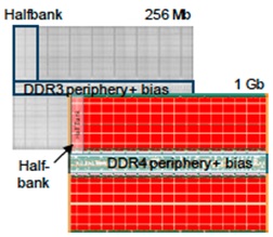
Fig. 1. Top down images of the Everspin 40nm 1.5 V DDR3 256 Mb (top) and the 1.2V DDR4 28nm 1 Gb (bottom) STT-MRAM product dies.
MRAM devices are implemented as magnetically-programmable resistors between two BEOL metal layers as shown in Fig. 2.
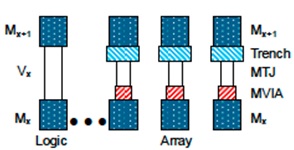
Fig. 2. Schematic diagrams showing integration of the pMTJ bits in the 1 Gb array and adjacent logic areas in the chip’s BEOL metallization.
The Magnetic Tunnel Junction (MTJ) consists of a fixed magnetic layer with high perpendicular magnetic anisotropy, an MgOx tunnel barrier and a magnetic free layer. Upon application of a critical voltage, a current of spin-polarized electrons tunnels through the MgOx barrier to flip the polarization of the free layer to be in a parallel or anti-parallel magnetic state, showing low or high resistance respectively to a read current. The free layer can be optimized for different applications. During write, no backhopping or switching abnormalities were observed indicating a large window for switching reliability for the industrial application temperature range from -35C to 110C. DIMM cycling indicated an endurance lifetime greater than 2e11 cycles. Fig. 3 shows data retention as a function of temperature of 10 years at 85C or 3 months at 100C.
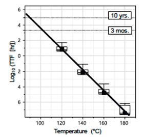
Fig. 3. Time to Failure vs. temperature for Data Retention (DR) bakes of a collection of 1 Gb dies. Solid line fit indicates DR of 10 years at 85°C and 3 months at 100°C.
2.2: 1 Gb High density Embedded STT-MRAM in 28nm FDSOI Technology
Lee et al, R&D Center, Samsung Electronics Co.
Based on the already shipping 8Mb 28nm FD-SOI eMRAM product, Samsung announces their embedded 1Gb product demonstrating read and write operation from -40C to 105C. For high performance and stable yield of over 90%, a temperature-compensated write driver and write assistor were implemented. Improved endurance up to 1e10 cycles was achieved to broaden eMRAM applications to eDRAM replacement. To guarantee high yield, 2b ECC was implemented. The MTJ stack is based on MgO/CoFeB. With an operating voltage of 1.0V and a 50ns read pulse, at an operating temperature from -40C to 105C, 10 years retention at 105C and endurance of 1e6 endurance cycles is demonstrated. The unit cell size is 0.036 um2 . MTJ stack engineering gave a higher TMR of over 200% and an improvement in MTJ efficiency (retention divided by switching current). Fig. 4 shows the vertical architecture and the TEM picture of the MTJ cell array.
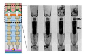
Fig. 4. Vertical structure and TEM images of MTJ cell array with Bottom Electrode Contact (BEC) embedded in 28nm FDSOI logic process.
Performance is illustrated by the room temperature shmoo plot in Fig. 5, showing the product spec VDD of 1.00V and the read pulse of 50ns.

The tuneability of the process to yield different products with 10-year data retention temperature and corresponding endurance is shown in Fig. 6.
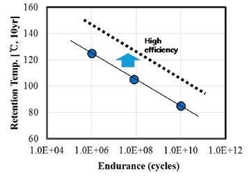
Fig. 6. Correlation between endurance and 10 year data retention temperature properties. With improved efficiency, retention temperature can be enhanced for the same endurance cycle.
2.3: 22nm FD-SOI Embedded MRAM Technology for Industrial-grade MCU and IOT Applications
B. Naik, et al, GlobalFoundries
The 40Mb, 0.8V embedded MRAM with 2b ECC achieved reliable operation from -40C to 125C with 5x solder reflows, 400C BEOL flows and 1e6 endurance cycling and stand-by magnet immunity of 600 Oe at 105C for 10 years. A high magnetoresistance (MR) ratio (Rap-Rp)/Rp where Rp is the parallel resistance or state ”0” and Rap is the anti-parallel resistance or state “1” and the figure-of-merit MR/s(Rp) resistance distributions are shown in Fig. 7.
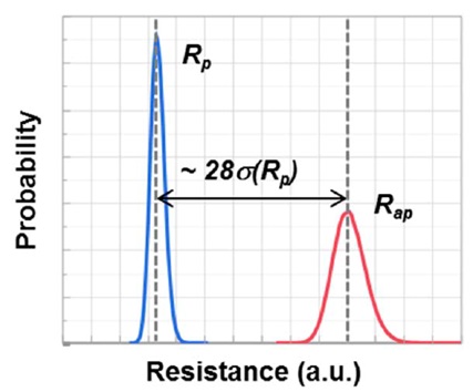
Fig. 7 Bit-cell resistance distributions of Rp and Rap showing separation of 28 s(Rp).
Write shmoo data for AP->P at 37 ticks and P->AP at 28 ticks for 200ns write pulse at 0.8V at -40C is shown in Fig. 8.
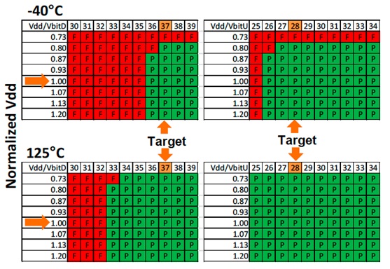
Fig. 8. Write shmoo for AP->P at 37 ticks and P->AP at 28 ticks for 200ns write pulse.
Read shmoo is shown in Fig. 9 showing operation at 19ns read pulse.
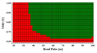
Fig. 9. Read shmoo showing read operation at 19ns.
Projected standby magnetic field immunity at 105C for 10 years is 600Oe. Standby magnetic field at immunity at 10 years as a function of temperature is shown in Fig.10.
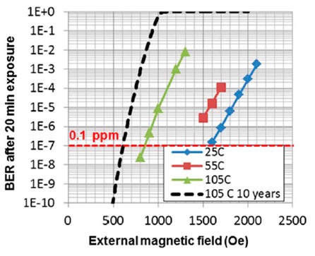
Fig. 10. Standby magnetic field immunity as a function of temperature.
In active mode, the magnetic immunity of 500 Oe is limited by the endurance margin.
2.4: 2 MB Array-Level Demonstration of STT-MRAM Process and Performance Towards L4 Cache Applications
Juan G. Alzate, et al, Intel Corporation
L4 cache-level application performance and reliability is shown for a 2 MB STT-MRAM array. This requires high density, high bandwidth and high endurance across industrial temperatures of operation. The required specifications for L4 cache application of an STT-MRAM are shown in Table I.
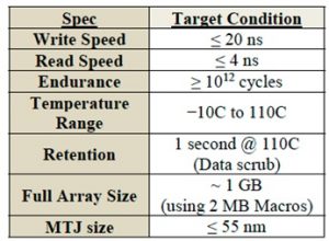
Table I. Target specs for STT-MRAM in an L4 cache application.
A bandwidth of >256 GB/sec and an array density of > 10Mb/mm2 are needed to be an SRAM or eDRAM replacement. The density requirement as shown in Fig. 11 limits the bitcell pitch and access transistor size and consequently restricts the maximum current available for STT write thus limiting the data retention time to *one second* at the maximum operating temperature of 110C.
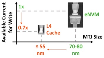
Fig. 11. Tighter bitcell pitch required for L4 cache compared to the eNVM application.
The write endurance requirement of 1e12 cycles on the other hand limits the maximum write current to ensure endurance fails remain within ECC-correctable limits. To achieve an acceptable ECC correctable 1 Gb array Bit Error Rate (BER) of <100 dpm (probability of 1Gb array fail of 1e-4), the required fixed and random Write Error Rate (WER) errors are shown in Fig. 12 for two different architectures, 128b words with Triple Error Correction (TEC) and 512b with Double Error Correction (DEC). The random BER needs to be 1e-8 to 1e-10 for 1e12 write events.
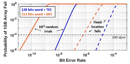
Fig. 12. ECC calculation for allowed BER of both fixed location fails (dashed) and random fails (solid) vs 1Gb array fail probability (ECC uncorrectable) assuming either 128b words with Triple Error Correction (TEC) (blue) or 512b words with Dual Error Correction(DEC) (orange).
The 55nm MTJ needs a reliable stack optimization and reactive ion etch (RIE) process. Defective fails were found to be shorting modes (hard shorts and soft shorts) that reduce the resistance and TMR. Failing bits at time=0 are fused out. Acceptable WER levels and shorter write pulses require overdriving the MTJ, limited by the available drive current and endurance considerations as shown in Fig. 13.

Fig. 13. Write current distributions limited by available drive current and endurance requirements and read disturb requirements.
The minimum current is that required by read disturb considerations and improves as temperature decreases, hence read disturb is measured at 95C by hammering full words with 1e7 reads. Write Error Rate curves are shown in Fig. 14 for MTJs scaled from the NVM application and the optimized L4 cache device with 10ns write pulse shown in blue.
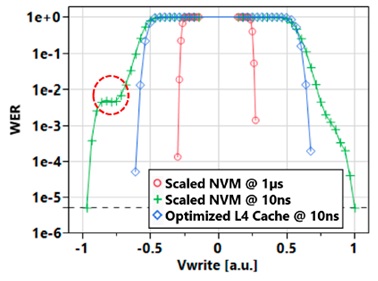
Fig. 14. Write Error Rates (WER) for different devices, showing the optimized L4 cache MTJ in blue.
The critical condition for WER is at -10C, but as temperature increases, MJTs become easier to write and at higher temperatures the VCC can be reduced. Endurance measurements are done at 105C due to thermal activation of defects causing MgO dielectric breakdown.
2.5: A novel integration of STT-MRAM for on-chip hybrid memory by utilizing non-volatility modulation
J.-H Park, et al, Semiconductor R&D Center, Samsung Electronics co. Ltd.
Samsung illustrates that it is possible to have either high-retention or high-speed STT-MRAM hybrid memory in separate zones in a single eight Mb chip in 28nm FD-SOI logic as illustrated in Fig. 15.
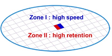
Fig. 15. Illustration of on-chip hybrid memory which can have two different sub-zones having MTJ arrays of modulated non-volatility: Zone I has relaxed non-volatility for high speed operation and Zone II has strict non-volatility for high retention requirements.
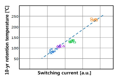
Retention was demonstrated at 10 years at 220C. For high-speed operation improvements were made in TMR, short fail probability, overdrive and write error rate. By tailoring the magnitude of perpendicular magnetic anisotropy (PMA) of MTJs without modifying the deposition process, the non-volatility in selected areas can be manipulated. Fig. 16 shows 10-year data retention temperature as a function of MTJ switching current.
To enable high-speed operation, wide read- and write margin are required. Read margin is increased by higher TMR at low RA by minimizing short failure. Two different MTJ processes, Process A and Process B are compared. Wider write margin is achieved by higher breakdown voltage (shown in Fig. 17), lower switching voltage, wider voltage margin between read and write and tighter distribution.
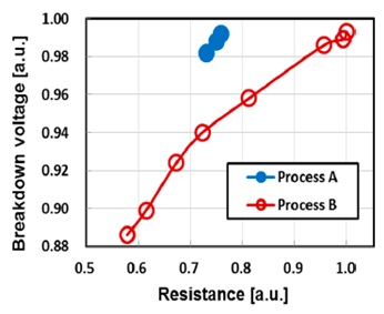
Fig. 17. Breakdown voltage as a function of MTJ resistance.
Fig. 18 shows write shmoo plots for 8Mb eMRAM macros integrated with the two types of MTJs of Process A and Process B , respectively. MTJs of Process A pass with much reduced write fail for the shorter pulse-width condition.
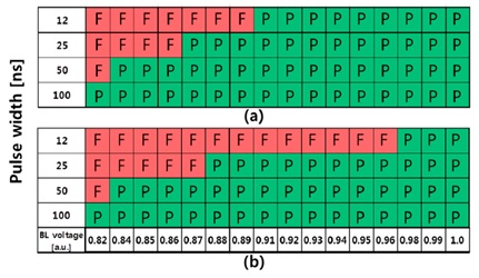
Fig. 18. Room temperature write shmoo plots as a function of pulse width and bitline voltage for two different processes, Process A (a) and Process B (b).
By implementing a highly tunable diversity of performances in a single chip as if multiple heterogeneous memories were embedded, both high performance and high retention memories can be implemented in the same chip, forming the hybrid memory. This is done by modulating the PMA energy to manipulate the non-volatility of MTJs.
2.6: Spin-transfer torque MRAM with reliable 2 ns writing for last level cache applications
Hu, et al, IBM-Samsung MRAM Alliance
Reliable 2 ns and 3 ns switching with two-terminal devices as opposed to the low-density, three-terminal SOT (Spin Orbit Transfer) devices, enables fast and dense MRAM products for Last Level Cache (LLC) applications. Reliable 2 ns switching was achieved for an STT-MRAM with 100% WER yield at 1e-6 write-error floor using 49nm CD MTJ.
In Fig. 19, switching current increases as pulse width decreases for two different free-layer designs, Stack1 and Stack2, annealed at 400C for 60minutes.
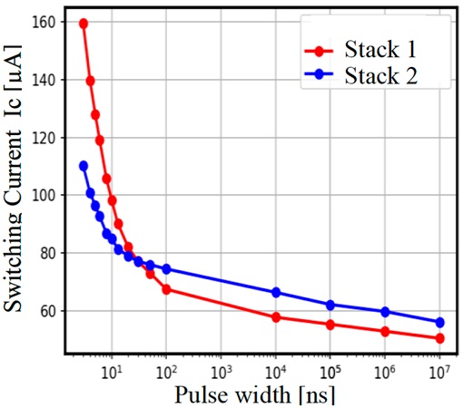
Fig. 19. Switching current vs pulse-width curves of two stacks with different free-layer materials each showing the thermally activated longer pulse width regime and the shorter pulse width of the precessional switching regime.
For long write pulses of 10 ns and above, the switching is thermally activated, but for short pulses of 10 ns and less, it is in the precessional switching regime governed by the conservation of electron spin angular momentum. LLC applications requiring write pulses <10ns operate in the precessional switching regime determined by the free-layer materials properties. The shorter pulse-width show steep increase of switching current, degradation of the WER slope and the occurrence of WER anomalies, all of which are addressed through materials optimization.
254 devices fabricated with free-layer type I having a nominal size of 49nm and median energy barrier Eb=55kT reached the required 1e-6 WER floor with 2 ns write pulses, illustrated in Fig. 20. A single device with CD=49nm and 2 ns write pulses reached the 1e-11 WER floor.
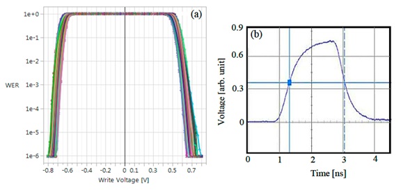
In a test of smaller 36nm MTJs, all 256 devices tested with 3ns write pulses reached the 1e-6 error floor and 242 of 256 devices tested with 2 ns write pulses reached the 1e-6 error floor for W0 operation while 228 reached the required error floor for W1 operation. Reference layer WER anomalies known as backhopping were observed.
2.7 22nm STT-MRAM for Reflow and Automotive Uses with High Yield, Reliability and Magnetic Immunity with Performance and Shielding Options
J. Gallagher, et al, Taiwan Semiconductor Manufacturing company
A 32Mb embedded STT-MRAM in 22nm was produced using a cell area of 0.046 um2 accommodating MTJs of varying CDs for different retention and performance requirements. The technology supports 6x solder-reflow-capability and -40C to 150C operation with data retention > 10years. The most recent process gave zero median t0 die bit fails per wafer as a result of the main improvement being the elimination of MTJ shorting defects. The main challenge for high yield at 150C is the reduction of the read window due to falling off of TMR with temperature, as shown in Fig. 21.
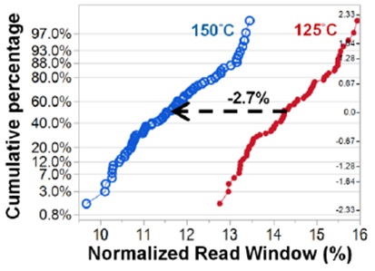
Fig. 21 Read window reduction due to falloff of TMR at temperature
Due to the stochastic nature of magnetic switching, write-verify-write is used, where the first shots incorporate lower amplitude write pulses both for power savings and for endurance stress minimization. If multiple low amplitude shots do not result in a successful write, final high amplitude write pulses may be needed to achieve high yields. At 25C all cells were written successfully with one shot whereas at -40C, 0-15% of the dice needed a second shot. Solder reflow reliability was demonstrated through six simulated reflow cycles, equivalent to 10 year retention at 225C. Since endurance has the highest failure rates at low temperature cycling, for 1e6 write cycles were tested at -40C, the resulting 0.029 ppm fails were within the 1 ppm margin for ECC. There was no change in parallel or anti-parallel cell read current distribution after 100K cycles at -40C as shown in Fig. 22.
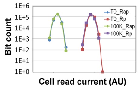
Fig. 22 Showing no change in either parallel (Rp) or anti-parallel (Rap) cell read current after 100K cycles
Read disturb rates showed < 1ppm for 1e12 cycles, as shown in Fig. 23 as a function of bitline bias voltage.
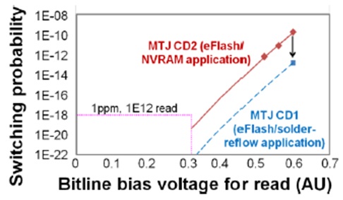
Fig. 23 Read disturb rates showed < 1ppm for 1e12 cycles, as a function of bitline bias voltage.
Investigations of magnetic immunity showed stand-by bit error rates for packaged MRAM arrays to be below 1ppm BER for 10-year exposures of 1100, 750 and 600 Oe at 25C, 85C and 125C respectively as shown in Fig. 24.

Fig. 24. Packaged MRAM arrays below 1ppm BER for 10-year exposures of 1100, 750 and 600 Oe at 25C, 85C and 125C respectively.
In-package shielding was used to protect against a tampering attack with a 3.5kOe magnet. Failure rates of an unshielded sample were ~30% after ~one second whereas the shielded part had <one ppm after 80hours at 25C for a reduction factor of >1e6 sensitivity.
Parts with smaller CDs were used for higher performance, trading off solder-reflow capability but still having very high retention >10 years at >150C. Tables II and III show read and write performance for a 0.038um2 cell. Table II shows read time and voltage shmoo at 125C showing a 6ns read cycle.
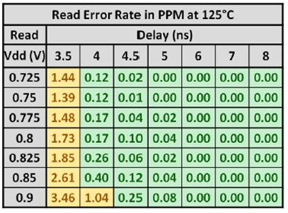
Table II. Shmoo showing read pulse width and bitline voltage at 125C
Table III shows bit line write voltage and programming pulse width shmoo for multi-shot programming at -40C. The smaller CDs achieved endurance of better than one ppm after 1e9 write cycles at -40C.
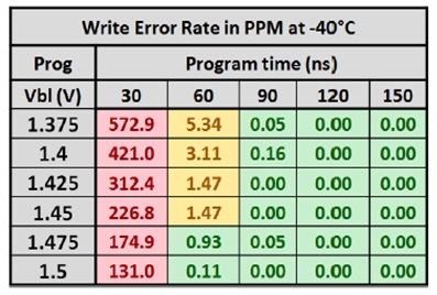
Table III. Shmoo showing bitline write voltage with pulse width for multi-shot programming at – 40C.
Share this post via:




Is Intel About to Take Flight?