From initial process technology development (TD) to high volume manufacturing (HVM) status for a new node, one of the key support functions to improve and maintain yield is the in-line wafer inspection technology. Actually, there are multiple inspection technologies commonly employed, with tradeoffs in pixel resolution, defect classification methods, and throughput.
At the recent SPIE Advanced Lithography + Patterning conference, Timothy Cummins, Senior Principal Engineer, and Kale Beckwitt, Principal Engineer, from the Yield, Logic Technology Development group at Intel, collaborated on a thorough review of the current status of inspection technology, in their talk, “SEM inspection for logic yield development and control”. (Although incoming bare wafer inspection is also a key function, the focus of their presentation and this article is on patterned wafer inspection employed in the fab.)
Metrology versus Inspection
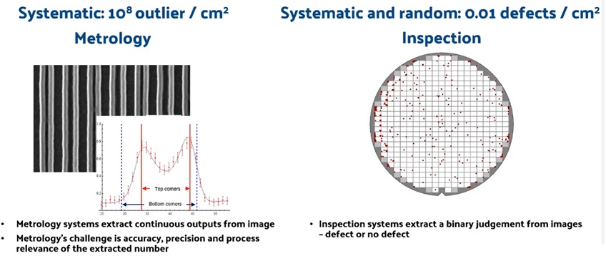
As a precursor to the discussion, Tim elaborated upon the difference between metrology and inspection. The figure below highlights the key features of the techniques.

Critical-dimension scanning electron microscope (CD-SEM) metrology data collection and analysis provide process development engineers with systematic, high-resolution measures of patterned wafer images. Additionally, metrology systems can assist with the defect density assessments over a very small field-of-view (FOV).
Inspection systems evaluate patterned wafers for the presence of systematic and random defects. In HVM, the goal is to assess whether the wafer-level defect density represents an outlier to the expected value.
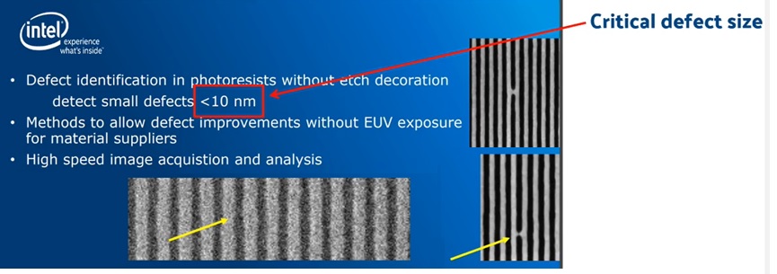
Tim indicated, “Both the scale of defects and defect size are factors in achieving process maturity. For example, current targets are ~5-10 defects per 300mm diameter wafer, with a critical defect size of 10nm.” (e.g., for a 200 mm**2 die size, 5K wafer starts per week in HVM). The figure below illustrates several facets of inspection.

Specific comments to highlight about the figure above include:
-
- the source of defects includes both fab operations and materials
(In addition to in-line wafer evaluation, incoming material inspection is also a key step.)
-
- inspection image acquisition methods are described in “giga-pixels per second” sampling rate
- the “signal-to-noise ratio” (SNR) in the image varies among different inspection technologies
The contrast between the foreground features of interest and the background “noise” may be limited, necessitating, additional software processing of the pixel data to identify potential defects.
Operational Requirements for In-Line Wafer Inspection
Tim provided the following guidelines for wafer inspection procedures:
-
- classification of both systematic and random defects
- a runtime target of “one hour per selected wafer” for yield control
- “full wafer” evaluation on a sufficient number of wafer samples to sustain HVM yield, on a fab running tens of 1000’s of wafers per month
Process line yield control requires measuring sufficient wafer area (e.g., 100’s of cm**2 per hour) to detect excursions from the target HVM defect density (e.g., 0.01 defects per cm**2).
OPWI and EBI Technologies
The two major categories of inspection equipment are:
-
- optical pattern wafer inspection (OPWI)
- electron beam inspection (EBI)
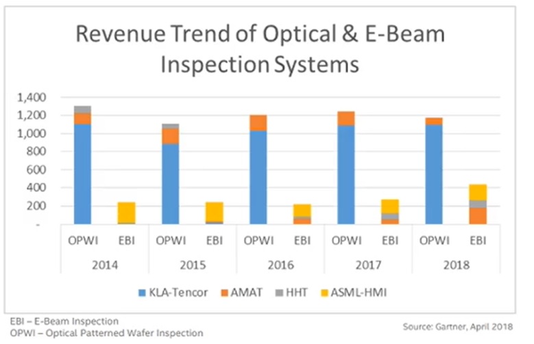
Tim highlighted the relative market share of these approaches, shown in the figure below (by equipment revenue, circa 2018).

Parenthetically, OPWI systems scan a light source across the patterned wafer. There will be a combination of reflected and scattered light from the wafer surface – a defect will contribute significantly to the scattered intensity. The light detector generates an image, which is compared against a reference, subtracting the two – a defect will be identified by the difference.
The goal for OPWI is to generate a high-resolution, high-contrast wafer scan image – the defect-related optical “signal” to background “noise” ratio (SNR) should be high. A brightfield inspection system places the detector in the reflected light path; the light source and detector are typically within ~45 degrees of normal incidence. A large field-of-view (FOV) and low required light intensity make brightfield analysis an attractive option. The loss of intensity due to scattering from a defect will shop up as a set of dark pixels in the bright background. Conversely, a darkfield inspection system places the detector away from the reflected beam to receive the scattered light; the light source is typically at an oblique angle to the wafer surface, between 0 and 45 degrees.
The scattering cross-section (SCS) of a defect increases (exponentially) with the defect size, while the SCS is inversely (exponentially) related to the source wavelength. To provide high-resolution images for smaller defect sizes, OPWI systems have had to incorporate shorter wavelength sources, transitioning from visible to UV to deep UV illumination.
The three main characteristics of the OPWI system are:
-
- the image resolution of the light source and detector
- the light scattering properties of the materials, and
- the resulting image contrast
The scattered light is a function not only of the presence of a defect, but also the refractive index and reflectivity of the (background) patterned materials. The (higher-order) optical diffraction angles from the background reflection increase as the CD of the patterned shapes is reduced. As a result, the noise in the image from valid patterns increases. Line edge roughness of a (valid) patterned line also contributes to noise, and a reduced SNR for defect detection.
Yield engineers strive to optimize the illumination wavelength(s), the illumination pattern (e.g., full-field, annular), and the light collection pupil plus detector design to improve the generated image for defect identification. (Note that a range of wavelengths may be used, given the strong wavelength dependence of the refractive index and reflectivity for the wafer surface materials.)
There are two OPWI approaches toward deriving the reference image for the difference calculation:
-
- comparison to an adjacent die
The reference could simply be the image from an adjacent die location to the die site being evaluated. A random defect present in the test site will almost assuredly differ from the image for a neighboring site. (Systematic defects in the two images may zero out and go undetected.)
-
- comparison to a reference model
At the expense of producing a model image for an expected “good” die, the test site image would be subtracted from this reference, known as a die-to-database comparison.
The alternative to optical reflection plus scattering technology is electron beam imaging, where an incident beam on a surface results in the emission of secondary electrons to be detected.
Tim described some of the characteristics of OPWI and EBI technologies for in-line yield monitoring applications.
-
- throughput
OPWI has maintained a prevalent presence for in-line defect detection due to the faster throughput:
-
-
- OPWI: ~20 gigapixels/sec @ 100nm pixel size
- CD-SEM EBI: ~20 megapixels/sec @ 1nm pixel size
-
Clearly, EBI would not provide sufficient throughput to be a complete yield development and control technology. Increasing the e-beam inspection current (and/or applying multiple adjacent e-beams) to improve throughput is limited by the Coulomb interaction between primary and secondary electrons.
-
- resolution
EBI offers improved direct resolution over OPWI, due to the optical diffraction limit. EBI also provides the opportunity for better contrast and defect detection across greater changes in wafer surface topography.
OPWI system developers are pursuing methods to improve resolution. Deep learning image post-processing algorithms may offer insights into defect images that are sufficient excursions from an image training set. One option for the training set would be to use a small range of values for each pixel around the median calculated over a large sample of images as the threshold for defect identification. As the wafer defects of interest are difficult to identify, a synthetic training set of images with both defects and low SNR contrast may be generated to guide the deep learning training phase.
Another option being pursued to improve defect identification with OPWI systems relates to the nature of the incident light. Rather than using the pixel intensity amplitude difference of two images, a polarized incident source beam will undergo a phase change upon reflection from the topography of the patterned surface. The presence of a defect will alter that phase change, which could be detected by darkfield ellipsometry.
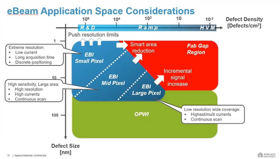
Kale shared the figure below, depicting the OPWI and EBI tradeoffs, with a gap region for the combination of HVM defect density and small defect size.

Although OPWI remains the workhorse inspection method, Kale highlighted applications where EBI techniques provide complementary support. The key technology that Kale focused on was voltage-contrast SEM inspection.
Briefly, VC-SEM utilizes the principle that a conduction element on the wafer surface with a voltage bias will alter the distribution of emitted secondary electrons when the beam is scanned. For example, a passive VC scan would electrically connect the wafer substrate to ground. A node on the surface that should be floating would acquire charge from the incident (low energy, <1keV) electron beam, achieving a negative potential. The floating node would thus emit more secondary electrons, and appear brighter in the VC-SEM scan. If the floating node were shorted to ground, few secondary electrons would be emitted resulting in a dark area in the VC-SEM. Differences between the images for an unconnected wafer and a VC-SEM grounded wafer connection can provide a means of defect inspection.
Additionally, a VC-SEM connection which should be grounded which is of high scan intensity is indicative of a floating node, likely due to a defective contact or via. Indeed, VC-SEM provides a class of defect identification which OPWI cannot.
Parenthetically, note that passive VC-SEM does not pinpoint the defect. It highlights an electrical issue associated with a circuit node. Further analysis of the physical layout is required for defect identification.
Active VC scanning goes further, applying patterns to the device under test to generate real-time SEM images. More sophisticated cabling/probing is required in the SEM vacuum chamber. Nodes at a non-varying potential during the pattern application will not change intensity in the scan. As before, differences between the sequence of time-based VC-SEM images of the DUR and a reference device are indicative of a defect.
About VC-SEM technology, Kale said, “VC inspection is limited to specific process layer and structure types. With careful experimental design, inline VC can have a 1:1 correlation to end-of-line fails.”
The throughput of VC-SEM relative to OPWI is still a concern, yet Kale offering the following comments about its applicability. “Test structures designed for defect mode-specific VC visibility give rapid yield and process window visibility.”
As shown in the figure below, he described a “design for inspection” methodology, with a unique standard cell layout that would be inserted as a filler cell during block placement, offering a significant amount of defect data per wafer.

Correspondingly, VC-SEM equipment manufacturers would provide multiple beam systems that can localize image capture over a subset of the full FOV, improving throughput.
Summary
Incremental advanced to both OPWI and EBI technologies continue to enable in-line defect inspection for technology development and HVM:
-
- improved optical and (multiple) e-beam sources
- computational advances benefit SNR and throughput (e.g., die-to-database modeling, deep learning algorithms)
- VC scan has high value for specific applications
However, Tim and Kale ended their presentation with the following observation:
“Throughput is the biggest need. A huge opportunity exists for the industry to provide disruptive solutions for higher throughput.”
A huge opportunity, indeed.
-chipguy
Also Read:
0.55 High-NA Lithography Update
Share this post via:


Comments
There are no comments yet.
You must register or log in to view/post comments.