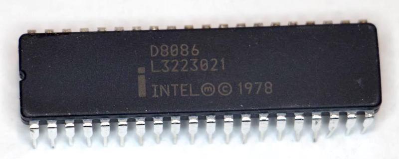
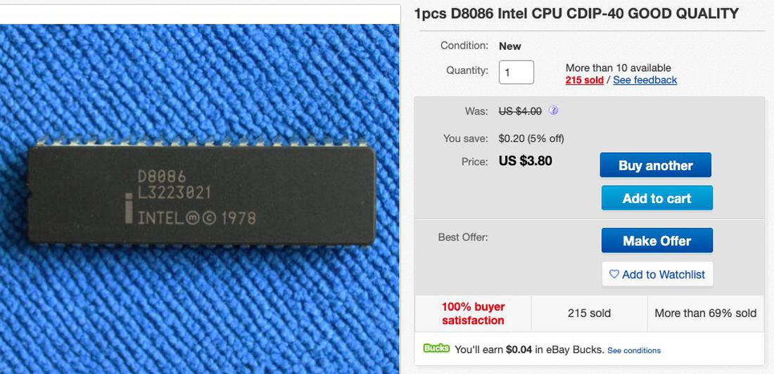
Intel introduced the 8086 processor in 1978, leading to the x86 architecture in use today. I’m currently reverse-engineering the circuitry of the 8086 so I’ve been purchasing vintage 8086 chips off eBay. One chip I received is shown below. From the outside, it looks like a typical Intel 8086.
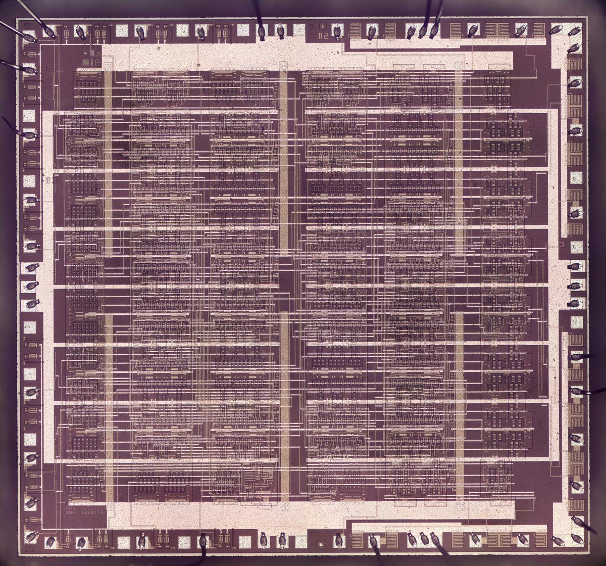
I opened up the chip and looked at it under the microscope, creating the die photo below. The whitish lines are the metal layer, connecting the chip’s circuitry. Underneath, the silicon has a purple hue. Around the outside of the die, bond wires connect the square pads to the 40 external pins on the IC.
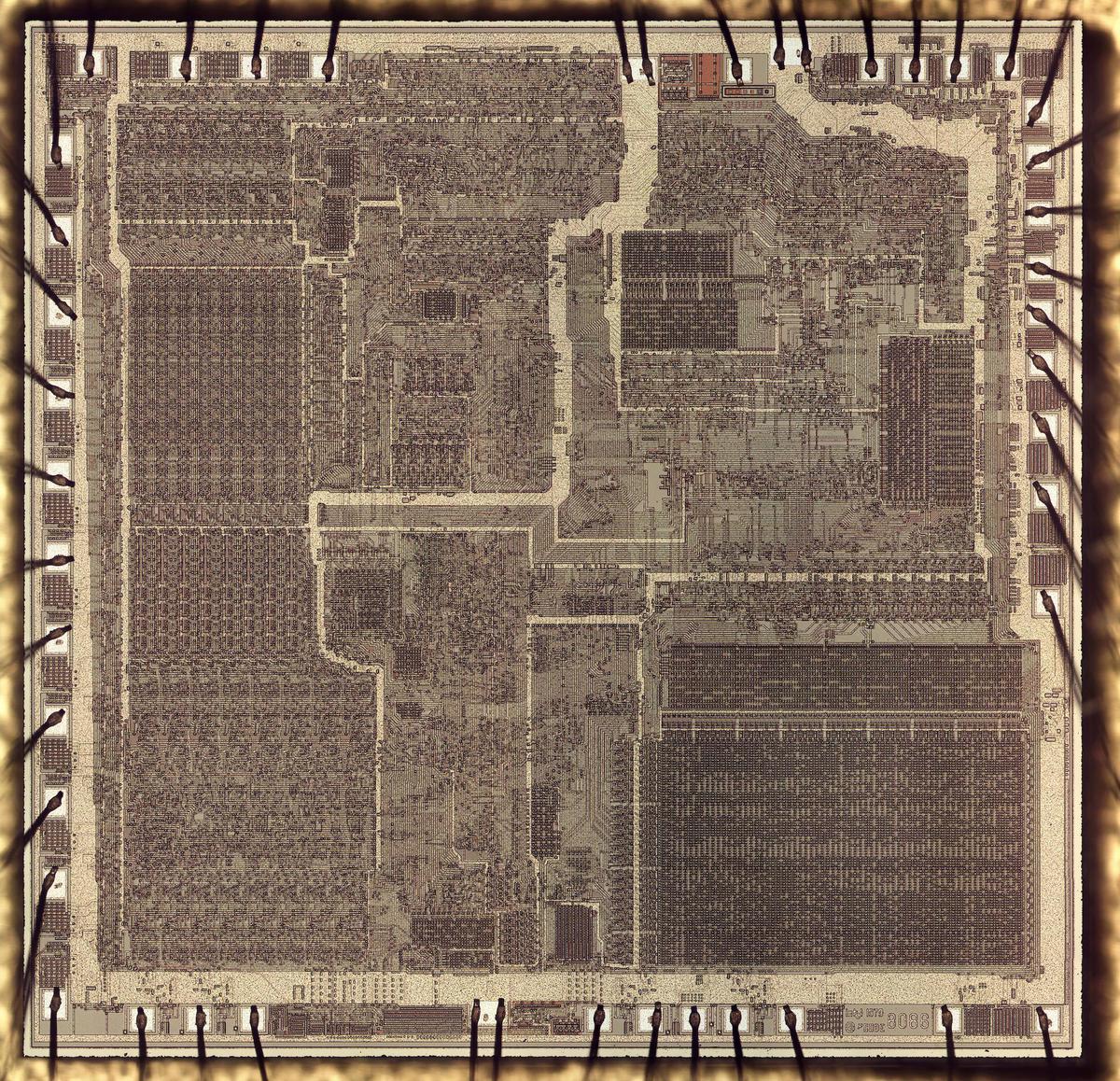
I quickly noticed, however, that this wasn’t an 8086 processor but something entirely different! For comparison, look at my die photo of a genuine 8086 below. As you can see, the chips are entirely different and the 8086 is much more complex. Someone had taken a random 40-pin chip and relabeled it as an Intel 8086 processor. The genuine 8086 has various functional blocks visible: the 16-bit registers and ALU on the left, the large microcode ROM in the lower right, and various other blocks of circuitry throughout the chip. (The genuine chip also has a tiny Intel copyright and the 8086 part number in the lower right. Click the image to magnify.) The fake chip above, on the other hand, is an irregular grid of horizontal and vertical wiring, with thicker horizontal and vertical lines for power.
The ULA or Uncommitted Logic Array
If the chip isn’t an 8086, what is it? I believe the fake chip is an Uncommitted Logic Array, a type of gate array. A gate array is a way of making semi-custom integrated circuits without the expense of a fully-custom design. The idea behind a gate array is that the silicon die has a standard array of transistors that can be wired up to create the desired logic functions. This wiring is done in the chip’s metal layers, which are designed for the customer’s requirements.2 Although a gate array doesn’t provide the flexibility of a fully-custom design, it was considerably cheaper and faster to design.
Ferranti invented the ULA in 1972, claiming that it was the first “to turn the logic array concept into a practical proposition.” A ULA allowed a single LSI chip to replace hundreds or even thousands of gates that otherwise would be implemented in a board full of 7400-series TTL chips. The most well-known users of a ULA are the popular Sinclair ZX 81 and ZX Spectrum home computers.3
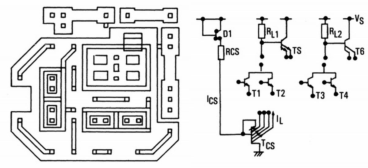
A ULA was based on a matrix of identical cells that were wired to form the logic gates. Around the edges of the chip, standardized peripheral cells provided the desired I/O capabilities. The diagram below shows a typical cell in the matrix. The cell contains multiple transistors and resistors, which are mostly unconnected by default. The ULA is customized by creating connections between the components to build a set of logic gates.
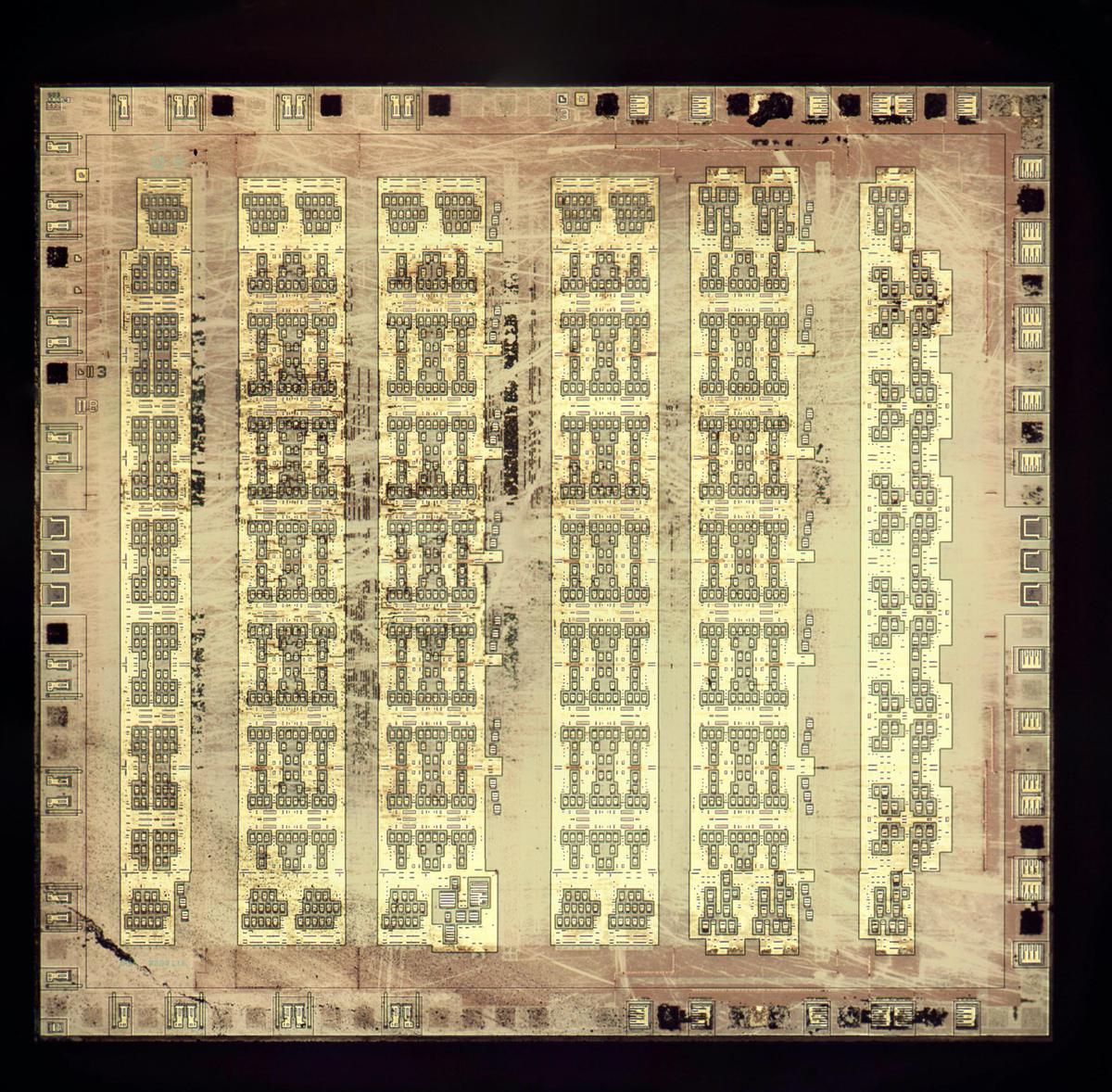
The photo below shows the fake chip with the metal layers removed, revealing the transistor array underneath. Each small green/yellow rectangle is a transistor; there are nearly 1000 of them. Note the repeated pattern of cells in the matrix,1 as well as the different peripheral cells around the outside. The density of transistors is fairly low; the chip has empty columns to provide room to route the metal layer.
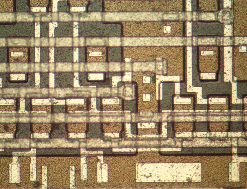
The fake chip uses bipolar transistors,4 completely different from the NMOS transistors in the 8086 processor. The closeup below shows transistors (the striped rectangles) and the two layers of metal wiring connecting them. (The genuine 8086 only has one metal layer, so the fake chip is probably more recent, from the 1980s.)
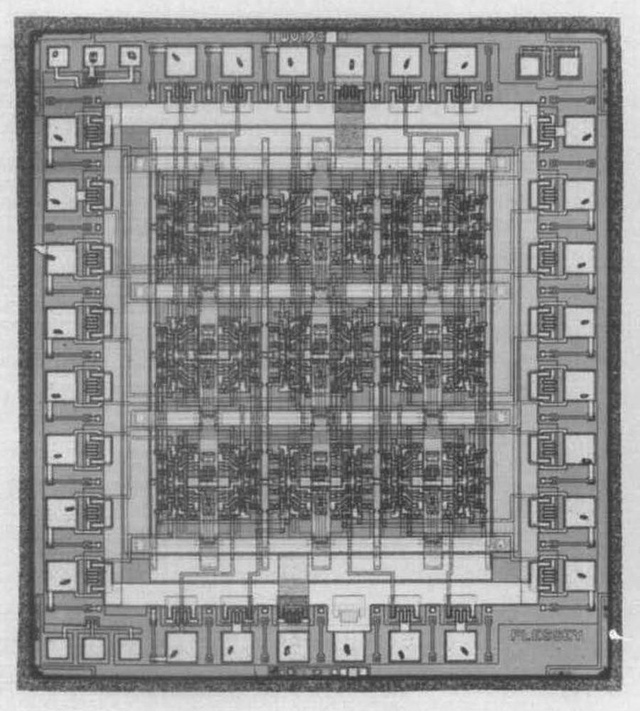
There is no manufacturer printed on the die of the fake chip. The matrix cells don’t look like the Ferranti cells. The photo below shows a ULA built by Plessey, another ULA manufacturer. That die has a smaller transistor matrix than my chip, but the overall structure is roughly similar, so Plessey might be the manufacturer.
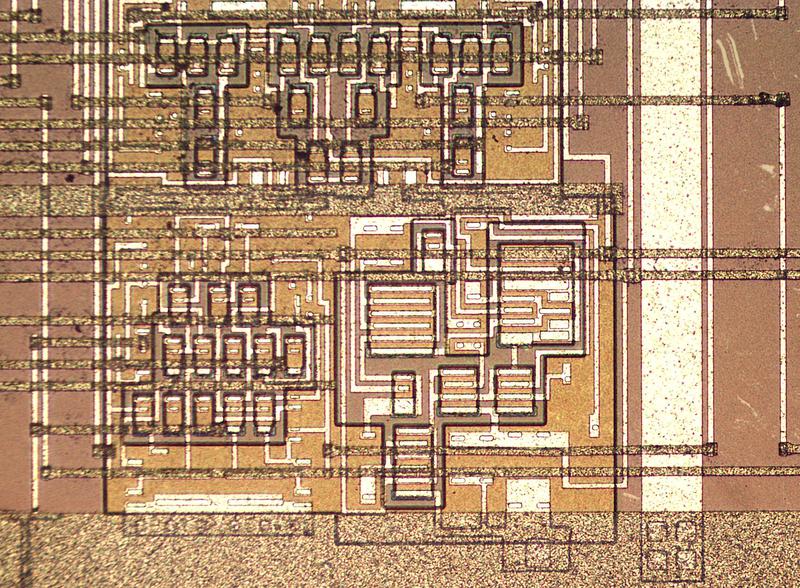
The photo below shows another detail of the fake chip. Matrix cells are at the top. The peripheral cell below has much larger transistors for I/O. (There are also resistors in the brownish regions, but they aren’t really visible.) The upper metal layer consists of horizontal wiring, while the lower metal layer is mostly vertical. The thick metal line at the right is for power (or perhaps ground) and is connected to a horizontal power distribution trace at the bottom.
To summarize, the position of the transistors and resistors in the ULA is fixed. This allows the same underlying silicon wafers to be manufactured for all the customers, keeping volume high and costs low. But by customizing the metal wiring layers, the ULA can be completed to fulfill the logic functions each customer needs.
Conclusions
Why would someone go to all the work of relabeling a $3.80 chip? I guess someone had a stack of old custom ICs with no value. By re-labeling them, they could at least get something for them. It hardly seems worth the effort, but I guess they make up for it in volume. The seller has sold over 215 of these 8086’s, although I don’t know if they were all fake or if I was unlucky. In any case, the seller gave me a prompt refund.
The seller’s feedback (below) shows a lot of complaints about fake chips. Even so, the seller’s feedback is 99.2% positive, so I suspect that there are just a few fake chips mixed in with many types of real chips. It’s also possible that most vintage 8086s are purchased by IC collectors who never test the chip.
I’ve been asked if this chip would actually work as an 8086. Sometimes counterfeiters sell a lower-quality chip in place of the real thing, such as the fake expensive op amps found by Zeptobars. But other times the fake chip is unrelated, such as the vintage bipolar RAM chips that I determined was a Touch-Tone dialer. Since an 8086 has 29,000 MOS transistors but the fake chip has under 1000 bipolar transistors, it’s clear that this chip won’t function as an 8086.
The moral is to always be careful when you’re buying chips, since you never know what you might find. Semiconductor counterfeiting is a big business and I’ve encountered just a tiny piece of it. I plan to write more about reverse-engineering the (real) 8086, so follow me on Twitter at @kenshirriff for updates. I also have an RSS feed.
Notes and references
- I think the fake chip has a matrix of 8×12 cells, with each of the large “IXI” patterns composed of four cells. ↩
- At first, a ULA was designed by hand by an engineer drawing the interconnects on paper, but by the 1980s, CAD software automated most of the design and testing. The CAD station below is pretty wild.
 CAD system for designing ULAs at Plessey. From “Computer Aided Design and New Manufacturing Methods for Electronic Materials”, 1985
 - The book The ZX Spectrum ULA: How to design a microcomputer discusses Ferranti ULAs in detail along with a complete explanation of the ULA in the ZX Spectrum. ↩
- Early ULAs used bipolar transistors, with CMOS circuitry introduced later. Different logic families were supported, depending on the needs of the application. Ferranti’s ULAs had three types of matrix cells: RTL (resistor-transistor logic), CML (current-mode logic), and buffered current-mode logic. Other ULAs supported fast ECL (emitter-coupled logic) or standard TTL (transistor-transistor logic).




Comments
6 Replies to “Inside a Counterfeit 8086 Processor”
You must register or log in to view/post comments.