Back in May, William Holt, EVP of technology and manufacturing at Intel gave a presentation to analysts entitled Advancing Moore’s Law, Imperatives and Opportunity. A pdf of the presentation is available here. I just saw it for the first time today and I’m not sure how to get my head around it. It starts off with a lot of historical stuff about how Intel has delivered process generations every couple of years (or maybe that the industry has, it’s not quite clear).
But the really interesting stuff is in the middle of the presentation. I have blogged before about how one of the challenges the semiconductor industry is facing going forward is that the cost per transistor is not coming down. Although there are more die per wafer at 20nm, 14/16nm etc, the cost of manufacturing that wafer is rising fast due to the increasing complexity of the process and, especially, due to the need for double patterning. The rule of thumb for a process generation in the past has been twice as many die per wafer (so a 50% reduction in area per transistor), but an increase of wafer cost by about 15% leaving 35% cost reduction left over.

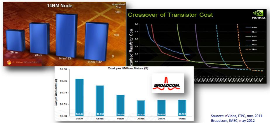
But going forward, the public information available up to now has either shown no reduction in cost per transistor or even a small increase. For example, the above montage, from an ASML presentation at Semicon in July, shows data from GlobalFoundries, Broadcom and nVidia. And at the common platform forum earlier this year Gary Becker of IBM in the press Q&A said that costs per transistor will come down but “the reduction will be less than we have been used to.”
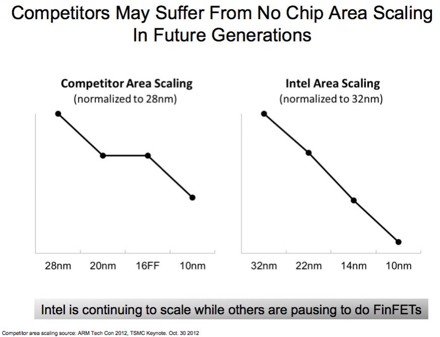
Both TSMC and GlobalFoundries 16/14nm processes basically have 20nm metal on top of a FinFET process, so there will be lots of speed/power improvements due to the improved transistors, but the effect on area scaling will be small.

As the above graph, from the Intel presentation shows, on the left there is a pause in area reduction (on the left) whereas Intel sees none since they have already done the heavy lifting to get FinFETs (that they call TriGate but I’m going to stick to the more generic term) into production at 22nm. But my understanding of Intel’s 22nm process was that it also was not aggressive on metal pitch to avoid double patterning, so I’m surprised they don’t show any flattening at all between 32nm and 22nm. Further, I suspect that the flatness of the competitor graph is exaggerated: even with the same metal pitch, faster transistors allow smaller standard cells to be used some of the time so I would expect to see some reduction in area.
As I said above, area reduction does not automatically result in a cost per transistor reduction since the cost per wafer may go up faster than the density comes down. This is especially true at 14/16nm when the metal does not shrink. Double patterning adds a to the cost for each layer that uses it. Twice through the stepper, and all the associated litho steps. For self-aligned double patterning, many more process steps to build the mandrel and remove it. But Intel sees none of this.

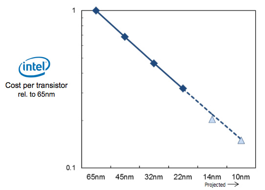
The cost per transistor is completely linear from 65nm down to 10nm despite the fact that at 65nm there is no double patterning and at 10nm there will need to be lots. And it is not an artifact of EUV, Intel have already said publicly that EUV is too late for 10nm.
I don’t understand how the above graph can be accurate. The cost per transistor is coming down completely linearly (actually, at 14nm they are predicting an even bigger reduction since the triangle is just below the line). As a presentation to financial analysts, this comes with all the caveats about forward looking statements, and clearly there may be unknown unknowns about 10nm. But no company is going to present data that is known to be false at the time it is presented, so I have to assume that this is an accurate (if simplified) view of Intel’s best estimate of their current and future costs.
I would like to know what TSMC, GF and Samsung think of these graphs. If they are true, Intel’s 14nm process has slightly better area than everyone else’s 10nm process (the top graph) and obviously hugely lower costs per transistor. I’m not sure I can believe it though.
Once again, Intel’s presentation is available here.
Share this post via:


Comments
0 Replies to “Intel Is Continuing to Scale While Others Pause”
You must register or log in to view/post comments.