On October 20 at the Linley Fall Processor Conference, GLOBALFOUNDRIES made a compelling case for designing smarter, not smaller AI chips. The virtual conference was filled with presentations on the latest architectures and chips for all types of AI/ML applications. It was therefore a refreshing change of pace to hear the fab technology view from GF. After all, without a fab everyone is just presenting simulation results.

Hiren Majmudar, vice president and general manager, Computing Business Unit at GF gave the presentation. Hiren has a strong command of the subject matter and gave a very well thought out presentation. He has a long career at Intel with some time at Magma/Synopsys and SiFive before joining GLOBALFOUNDRIES.
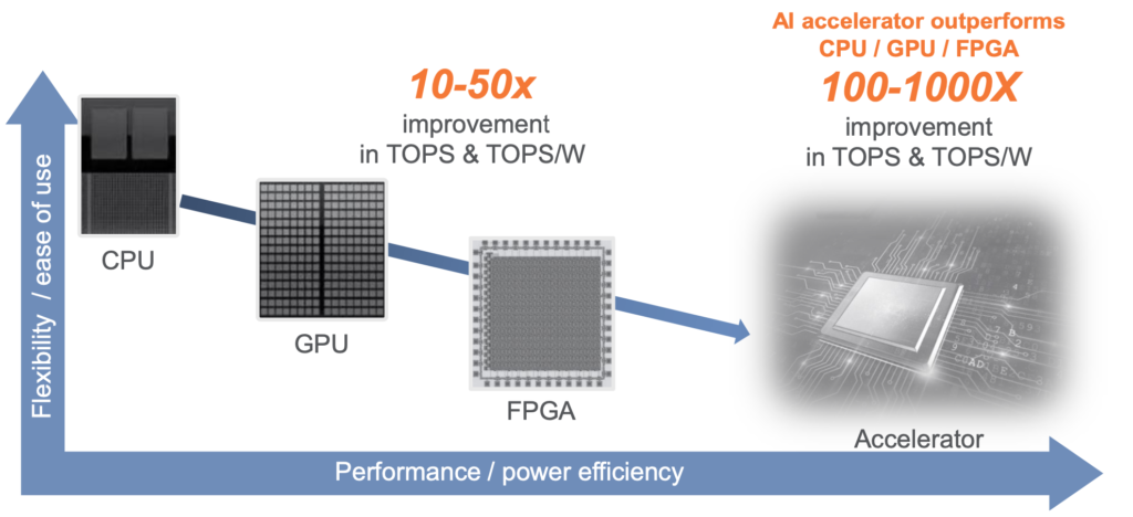
Hiren began with data from ABI Research showing a substantial rise in ASIC TAM for the AI silicon market over the next few years when compared to GPU, FPGA and CPU. I have a long history in the ASIC market, so Hiren was singing my song. At the end of the day, a purpose-built ASIC accelerator will out-perform all other approaches by a substantial margin. Hiren presented a nice graphic that drives the point home.

Next, Hiren discussed a couple of very relevant trends that are well-known. Moore’s Law is slowing at advanced nodes, so cost reduction and speed improvement aren’t what they used to be. At the same time, Dennard’s Law has stopped working, so power is no longer reduced by moving to an advanced node either. Hiren then proposed the solution to all this – use domain-specific architectures that address performance and power needs with custom approaches and build them on an optimized process for the problem at hand. Two GF platforms were presented as fitting the model quite well:
- 12LP/12LP+ (FinFET), which delivers excellent performance/watt, and improves total cost of ownership while enabling optimal return on investment
- 22FDXR® (FD-SOI), which offers the highest TOPS/W for power constrained solutions, economically
Hiren offered some examples of how these platforms are being used. For cloud and edge servers, performance/watt for training and inference is important as these are high performance applications. Two customer applications using 12LP/12LP+ are:
- Tenstorrent , with 368TOPS in a 75W PCI-E FF
- Enflame, who has packaged 14B transistors in advanced 2.5D
For edge devices, low power inference is key as most of these applications are battery powered. Two customer applications using FD-SOI from GF are:
- Perceive, with a massive number of neural networks in a 20mW envelope with no external RAM
- Greenwaves, who is achieving 150 giga ops at 0.33 mW/GOP
Regarding FinFET, Hiren discussed their power optimized SRAM. Memory is a critical building block for AI applications. He also mentioned GF’s design technology co-optimization where GF will work with the customer. He also described GF’s dual work function gates, which deliver several advantages:
- Lower variability
- Analog matching
- SRAM Vmin
- Improved derate in AOCV
- Less gate induced drain leakage (better static power)
- Better mobility (better drive)
- Lower junction cap (improved AC performance)
An AI-focused logic library and memory structures are also provided, and there is a third-party IP ecosystem for the technology as well.
Hiren described the fully-depleted silicon on insulator 22FDX technology as FinFET-like. This technology delivers many of the benefits of FinFET in a simpler bulk technology. Thanks to GF’s unique body bias ecosystem, ultra-low leakage designs are possible. The technology is useful in the automotive sector for ADAS applications. GF’s MRAM technology also helps here to deliver low power and low latency.
Hiren concluded with some more color about how GF partners with their customers to deliver optimized chips that target specific AI workloads. It was clear that designing smarter, not smaller AI chips is a winning strategy with GF. You can learn more about GF’s 12LP technology here and their 22FDX technology here. You can also get the views of Linley Gwennap, Principal Analyst, The Linley Group in his piece entitled Building Better AI Chips.
Also Read:
The Most Interesting CEO in Semiconductors!
GLOBALFOUNDRIES Goes Virtual with 2020 Global Technology Conference Series!
Designing AI Accelerators with Innovative FinFET and FD-SOI Solutions
Share this post via:


Musk’s Orbital Compute Vision: TERAFAB and the End of the Terrestrial Data Center