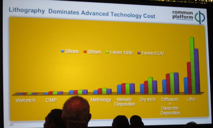
 As you know, I’ve been a bit of a bear about what is happening to wafer costs at 20nm and below. At the Common Platform Technology Forum last week there were a number of people talking about this in presentations and at Harvey Jones’s “fireside chat”.
At the press lunch I asked about this. There are obviously lots of technical issues to address to get to 10nm and below, and I don’t want to underestimate them, but at some point an important question is “at what cost.” Historically, with each process generation we have had something like a 50% reduction due to scaling along with a 15% increase in wafer fabrication cost resulting in an overall 35% reduction in cost per transistor.
Mike Noonen of Global Foundries answered the question. But like that dog in Sherlock Holmes that didn’t bark, Mike didn’t say the costs are going down. He talked about the value of moving to more advanced process nodes: higher performance, lower power. This is all true, of course, and for some markets the value is enormous (smart phones and data center servers most obviously). However, we are clearly entering a new era where we don’t get everything for free anymore. Nobody knows what will happen to Moore’s law in practice when we don’t get more transistors, faster designs, lower power designs, and it’s all cheaper. Instead, it is “how much extra would you pay for lower power?”.
Later, Gary Patten of IBM was more explicit. “Yes,” he said, “there is a cost benefit but it is much smaller that we have been used to.”

The problem is lithography (see the picture, litho is on the right). Even the purple bar on the right, which is EUV, doesn’t really get those costs completely under control.
In Handel Jones’s fireside chat with Brian Fuller, he said that they have done significant work to show a reduction in cost. He said that the big issue is parametric yield, mostly related to leakage. Some yield is driven by defects in processing and, while there is always some learning to be done, that is under control. But at these advanced nodes, with high variability, the issue of yield needs to be optimized at the design stage or parametric yield loss will make render the design financially non-viable.
Handel reckoned that design closure costs doubled from 45nm to 28nm and are double again from 28nm to 20nm. Leakage is the killer and the designs need to be optimized for it.
The other challenge at these advanced nodes is the volume required to make a design economic. Handel’s numbers are a cost of $100M/design at 20nm meaning a market of $1B or more for that design. Only 4 or 5 companies (Apple, Samsung, Intel…) can cope with this but the volumes will be very high.
Even Intel is not immune. At the press lunch someone pointed out that Intel’s costs had gone up 30% from 32nm to 22nm and it had taken them 24 months to get them down and under control. And of course, they play in a market with very high margins and where performance is valued very highly. That won’t work for more cost-sensitive markets.
If you read articles about electronics in the non-specialist press (aka newspapers, Time, the Economist etc) everyone assumes that electronics is going to continue getting cheaper. But we may be in a different regime. Yes, your smartphone will have longer battery life and do amazing voice recognition and so on. But it won’t get much cheaper than it is today (today meaning that most of the expensive components are manufactured on 28nm). But wait, it gets worse. If all that voice recognition requires twice as many transistors for all those processor cores then the cost of that chip may be close to twice as much as the old one. This is not what we are used to.
Share this post via:


Musk’s Orbital Compute Vision: TERAFAB and the End of the Terrestrial Data Center