You are currently viewing SemiWiki as a guest which gives you limited access to the site. To view blog comments and experience other SemiWiki features you must be a registered member. Registration is fast, simple, and absolutely free so please,
join our community today!
I attended the Jasper User Group this week, at least the keynotes, the first by Kathryn Kranen the CEO of Jasper and the second by Bob Bentley of Intel.
Kathryn went over some history, going back to when the company was started (under the name Tempus Fugit) back in August 2002 with a single product for protocol verification. Now, since… Read More
Verification and AMS are top search terms on SemiWiki so clearly designers have a pressing need for fast and accurate verification of today’s mixed-signal SoCs that include massive digital blocks and precision analog/RF circuits. They need simulation performance to verify the mixed-signal functionality, and they need nanometer… Read More
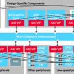
We have shown in Semiwiki how strong Cadence position was in Verification IP (VIP) in a previous post focusing on Interface standards like SuperSpeed USB or PCI Express. But IP based functions are used everywhere in a SoC, not only to interface with the external world, and need to be verified, as well, like for AMBA based functions.… Read More
One technology that has quietly gone mainstream in semiconductor design is FPGA prototyping. That is, using an FPGA version of the design to run extensive verification. There are two approaches to doing this. The first way is simply to build an prototype board, buy some FPGAs from Xilinx or Altera and do everything yourself. The… Read More
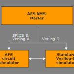
Analog Mixed-Signal (AMS) behavioral models have not caught on with the AMS designer community. Why? I suspect a significant reason (but certainly not the only one) is the way they are presented.
First, what is AMS behavioral modeling?
I define it as “a set of user-defined equations that decribe the terminal behavior of a component”.… Read More
Modern SoC (System On Chip) designs contain a larger number of RAM (Random Access Memory) instances, so how do you know what the speed, timing and power are for any instance? There are a couple of approaches:
[LIST=1]
Trust the IP supplier to give you models that use polynomial equations to curve-fit the performance numbers based…
Read More
The weather in Taiwan last week was very nice, not too hot but certainly not cold. The same could be said for the TSM stock which broke $16 after the October financial report where TSMC reported a sales increase of 15% over September. Revenues for this year thus far increased 19% over last year so why isn’t TSM stock at $20 like I predicted… Read More
The numbers for smartphone sales in Q3 are starting to roll in. These are in units and not yet revenue (let alone profit) numbers although everyone down to Sony is for sure profitable. Samsung is running away with the volume, selling more than Apple, Huawei and Sony put together. One name that is missing is Motorola (Google) which … Read More
As George E.P. Box said, “essentially all models are wrong but some are useful.” That is certainly the case with Carbon’s models. For processors they have two models, one that is fast (but not timing-accurate) and one that is accurate (but not fast). But both are useful.
Carbon attended the ARM TechCon in Santa… Read More
At ICCAD earlier this week, CEDA sponsored a talk by Alberto Sangiovanni-Vincentelli looking back over the last 30 years (it is the 30th anniversary of ICCAD) and looking to the future. As is always the case in these sorts of presentations, the retrospective contained a lot more detail than the going forward part. Clayton Christensen… Read More


Enhancing Multi-Domain System Simulation with FMI Co-Simulation