You are currently viewing SemiWiki as a guest which gives you limited access to the site. To view blog comments and experience other SemiWiki features you must be a registered member. Registration is fast, simple, and absolutely free so please,
join our community today!
In an environment of SoCs with tough targets of multiple functionalities, smallest size, lowest power and fastest performance to achieve within a limited design cycle window in order to meet the rigid time-to-market requirements, any day spent without success becomes very frustrating for a designer. Especially during tape-out… Read More
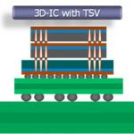
Two conferences on 3D, one just over and one coming up next week. The one that was just over was hosted by Georgia Tech, the 3rd Annual Global Interposer Technology Workshop (GIT). I wasn’t there but my ex-colleague from VLSI Technology Herb Reiter was. Herb has become very much associated with all things 3D since he led the … Read More
I came across an interesting article by Will Strauss which is pretty much the history of DSP in communication chips. Having lived through the early part of the history while I was at VLSI Technology I found it especially interesting.
At VSLI, our first GSM (2G, i.e. digital not analog air interface) was a 5-chip chipset. The DSP functionality… Read More
The MOS-AK/GSA Modeling Working Group, a global compact modeling standardization forum, delivered its annual autumn compact modeling workshop on Sept. 20, 2013 as an integral part of the ESSDERC/ESSCIRC Conference in Bucharest (RO). The event received full sponsorship from leading industrial partners including Agilent… Read More
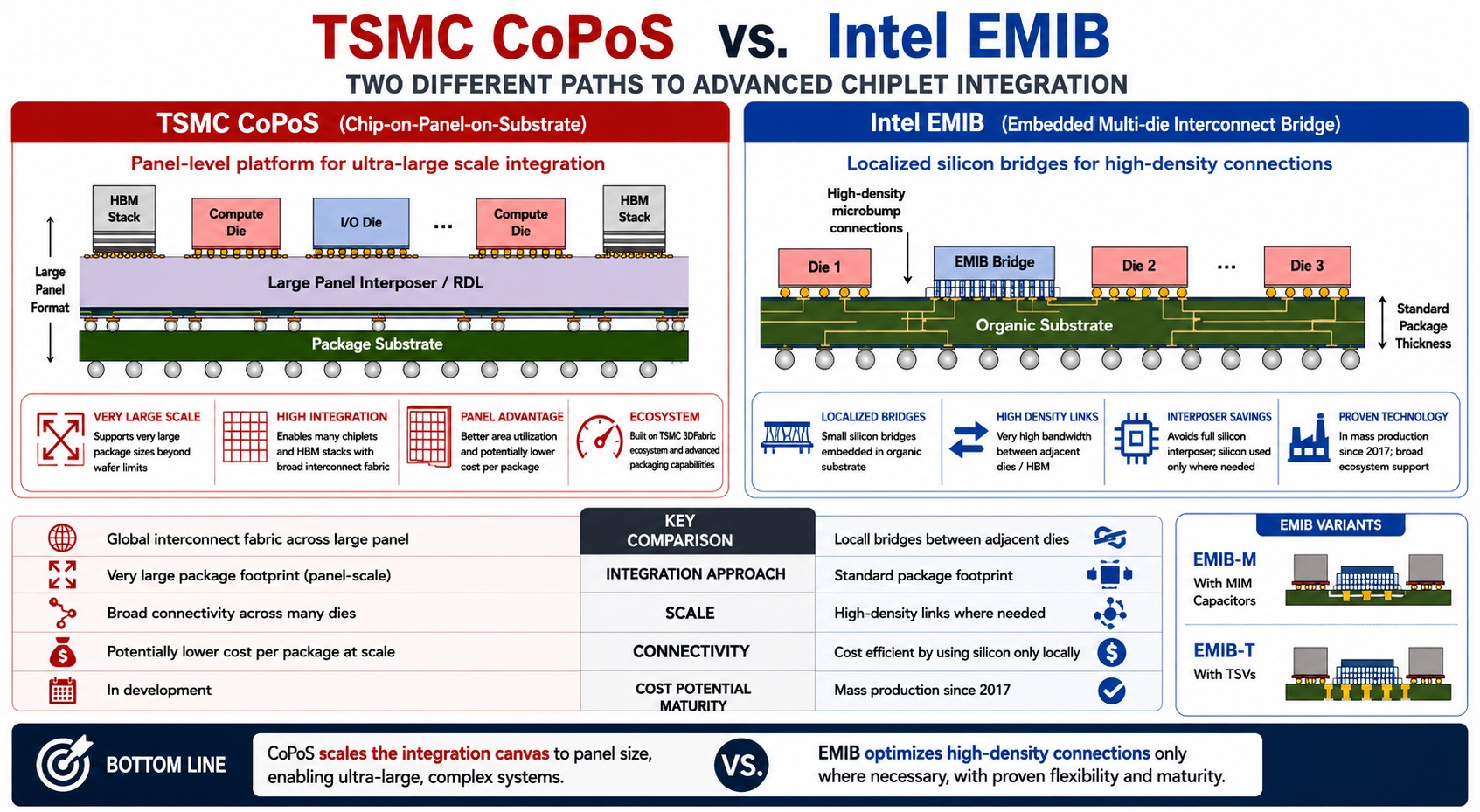
Hopefully this blog will result in a meaningful discussion on truth and transparency, and how Intel can do better in regards to both. Take a close look at the manufacturing slides presented by William Holt, Executive Vice President General Manager, Intel Technology and Manufacturing Group. You can see the slide deck HERE. Slide… Read More
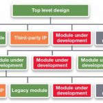
Now a day, a SoC can be highly complex, having 100s of IPs performing various functionalities along with multi-core CPUs on it. Managing power, performance and area of the overall semiconductor design in the SoC becomes an extremely challenging task. Even if the IPs and various design blocks are highly optimized within themselves,… Read More
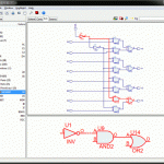
We cordially invite you to attend this webinar and learn how to quickly debug post layout designs. Concept Engineering is a privately held company based in Freiburg, Germany. It was, founded in 1990 to develop and market innovative schematic generation and viewing technology for use with logic synthesis, verification, test … Read More
To the surprise of nearly all observers and due to no extraordinary technological advancement, there is one true mobile winner of the past year and that is Micron, whose stock has soared in 2013 from $5 to $21. I know, you’re probably saying, “Micron, you can’t be serious.” Let’s run through the … Read More
SystemVerilog as an assertion language improved and simplified with the 2012 version compared to the 2005 version. I recently viewed a webinar on SystemVerilog 2012 by consultant Srinivasan Venkataramanan, who works at CVC Pvt. Ltd. There’s been a steep learning-curve for assertions in the past, and hopefully you’ll… Read More
FPGA design today involves not only millions of gates on the target device, but thousands of source files with RTL and constraints, often generated by multiple designers or third party IP providers. With modules organized in some logical way describing the design, designers brace themselves for synthesis and a possible avalanche… Read More


Previewing FMS 2026: The Next Frontier of Enterprise Memory, CXL, and AI-Era Storage