You are currently viewing SemiWiki as a guest which gives you limited access to the site. To view blog comments and experience other SemiWiki features you must be a registered member. Registration is fast, simple, and absolutely free so please,
join our community today!
The hottest real estate? Your wrist!by Beth Martin on 12-19-2013 at 3:28 pmCategories: General
I first read about the Pebble smartwatch earlier this year and thought “I don’t need yet another electronic device, and certainly not one that’s attached to my body.” Then I felt bad. Am I a troglodyte? It’s true, I do still have an iPhone 4, which is a little embarrassing in Silicon Valley. I have also never worn a wrist watch of any kind,… Read More
I spend about an hour a day reading blogs from EDA companies, foundries, independent bloggers and of course, SemiWiki. Richard Goering at Cadence assembled a top 10 list of the most popular blogs posted on their site in 2013, revealing that engineers were most interested in: FinFETs, 20nm and smaller nodes, memory technology and… Read More
The first keynote at the Burlingame 3D conference was by Doug Yu of TSMC. Not surprisingly he was talking about 3D. In particular, TSMC has WLSI technology that they call CoWoS, which stands for chip-on-wafer-on-substrate which pretty much describes how it is built. This is the technology that Xilinx uses for its recently announced… Read More
We have posted several blogs related to Cadence IP strategy, or I should say new strategy. Each of these blogs was dealing with a particular product, like PCI Express gen-3 Controller IP, latest DDR4 Memory Controller or Wide I/O. This approach was equivalent to describe trees, one after one, and finally ignoring the forest! It’s… Read More
It was a dinner with more than a thousand semiconductor professionals from around the world keynoted by Author and Editor in Chief of Forbes Magazine Steve Forbes. What more could a humble blogger ask for? Even at $250 a plate it was well worth it just to mingle amongst the people who make this industry so great.
Global Semiconductor… Read More
Yes, it is that time of year again, DAC is coming and it is in San Francisco so you can bet we will break attendance records, absolutely. I would like to call on ALL semiconductor IP companies to exhibit this year. IP is the center of the semiconductor design universe, DAC is the premier semiconductor design event, and San Francisco … Read More
It is that time of year and once again Atrenta has produced a video wishing you all the best for the holiday season. They are so spread around the world it is not just Hanukkah and Christmas but the Asian Lunar New Year (end of January) and probably some more holidays I don’t even know about. Last year there was a competition to name… Read More
Formal approaches and security are a perfect match since you really want to prove that there are no holes in your security, rather than just being fairly confident. At the recent Jasper User Group meeting, Victor Purri presented some case studies in security verification.
The Jasper Security Path Verification (SPV) App is used… Read More
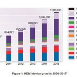
High Definition Multimedia Interface (HDMI) is today part of our day to day life, at home as well as at our office we are using devices integrating HDMI ports. HDMI penetration is well illustrated by this picture (created in Dec. 2011 by In-Stat): from DTV to Game console, the devices belong to the Consumer Electronics market segments,… Read More
This has been a heated topic since Intel announced that it would open its manufacturing facilities to the fabless ecosystem more than a year ago. I for one think it is a colossal mistake and I’m not surprised that many others share this view. IDM’s offering of excess manufacturing capacity to semiconductor design companies… Read More


Enhancing Multi-Domain System Simulation with FMI Co-Simulation