You are currently viewing SemiWiki as a guest which gives you limited access to the site. To view blog comments and experience other SemiWiki features you must be a registered member. Registration is fast, simple, and absolutely free so please,
join our community today!
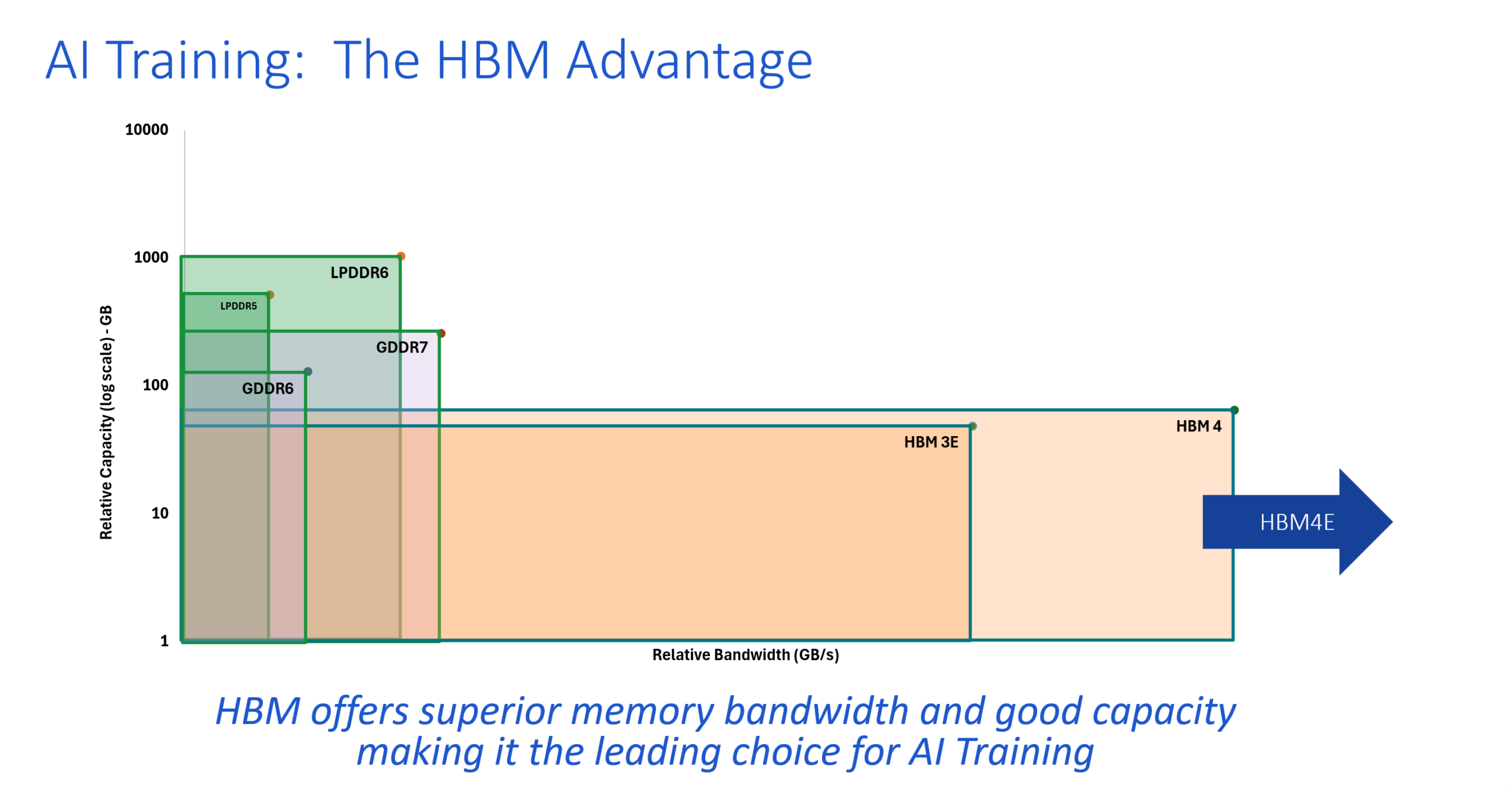
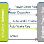
If it has escaped your notice that power management on SoCs is important then you need to get out more. Increasingly, the complexity of the interconnect between the various processors, memories, offload processors, devices, interfaces and other blocks means that the best way to implement it is to use a network on chip (NoC). But… Read More
Today at the Semisrael Expo 2013 (in Israel of course) Ajoy Bose gave a keynote on how design methodology will impact electronics. The big pictures is that microelectronics is driven by some major disruptive forces and, as a result, technology and industry are evolving dramatically, which creates a need for research and innovation… Read More
This fall there seems to be a bumper harvest of cores. Today Imagination Technologies announced their latest core for image signal processing. Like all of their cores, it is designed to be part of an SoC and is designed to work with other Imagination cores to build a complete image processing system. In particular, it is designed … Read More
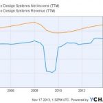
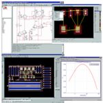
In the third and final (for now) part of this series on the EDA design tool vendors, I’d like to take a closer look at Cadence Design Systems. This is probably the most interesting of the three from both an industry perspective as well as an investment perspective for a variety of reasons. With that said I’d like to first provide some … Read More
eSilicon Corporation was founded in 2000 with Jack Harding as the founding CEO and Seth Neiman of Crosspoint Venture Partners as the first venture investor and outside Board member. They both remain involved in the company today, with Jack continuing as CEO and Seth now serving as Chairman of the Board.
Both Harding and Neiman brought… Read More
When I talk about social media and mention Synopsys you may quickly think of Karen Bartleson, the Senior Director of Community Marketing, because she:
…
Read More
TowerJazz and Silvaco BFFby admin on 11-15-2013 at 1:04 pmCategories: EDA
Last week was the TowerJazz Technology Fair 2013. TowerJazz is the fourth biggest foundry in the world after TSMC, GF and UMC. They have fabs in Newport Beach (the old Jazz, itself with roots in Rockwell), two in Israel (the old Tower, with roots in National Semiconductor) and one in Japan (acquired from Micron). The technology fair… Read More
In fact KitKat advocates low-power always-on functionality, and this is essential for contextual-awareness. Always-on functionality is saving battery life, which seems to be weird at first: if your phone is always-on you would expect it to consume much power… But always-on goes together with screen-off (the screen is a high… Read More
Cadence’s Signoff Summit will be held next week, November 21 at Cadence in San Jose.
This is the first of a series of all-day Signoff Summits from Cadence that focus on the multiple facets of design signoff. This first summit will include keynote addresses plus sessions covering the multiple solution components that comprise… Read More
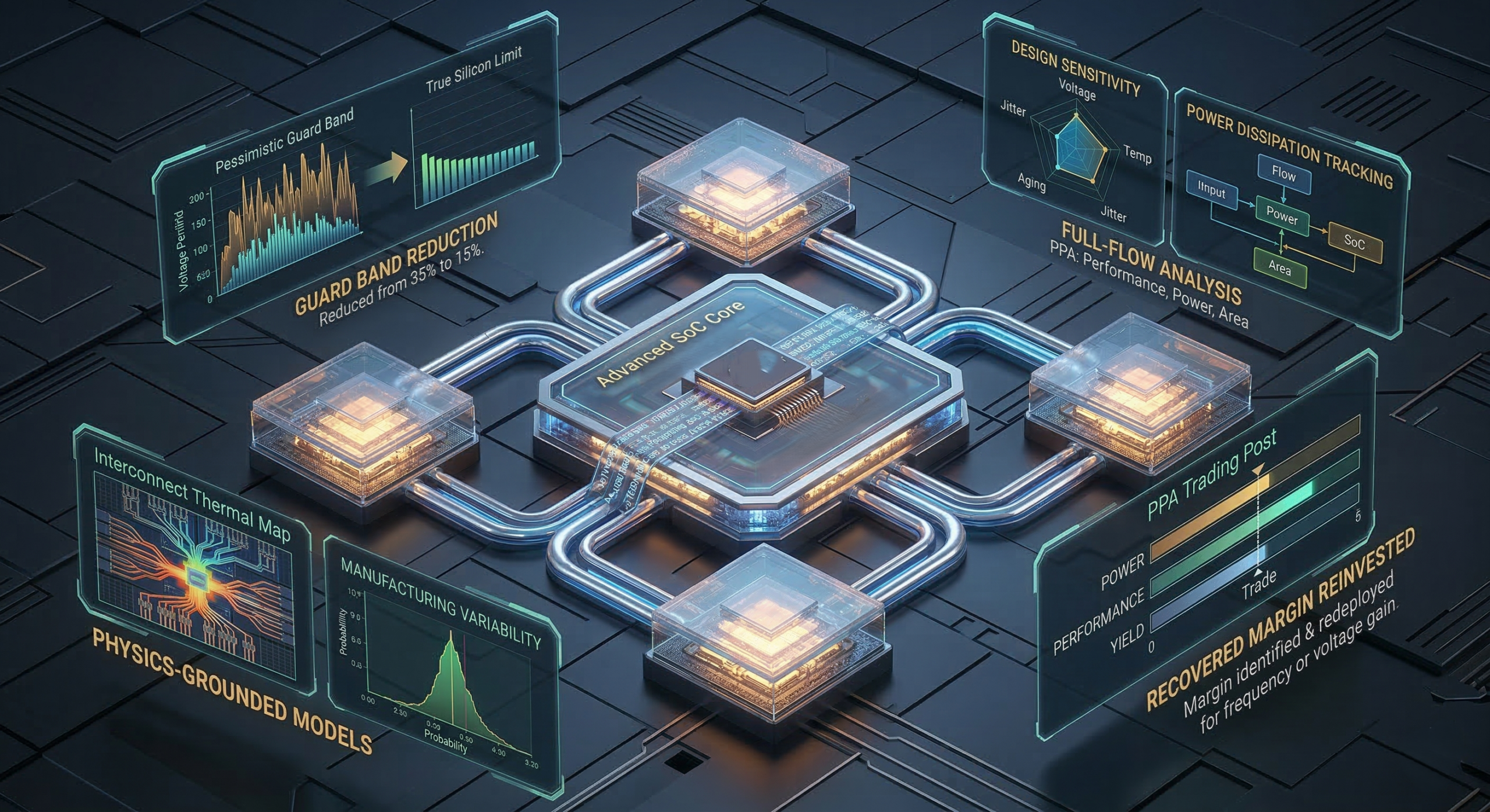
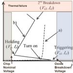
As Moore’s law keeps going, semiconductor design density on a chip keeps increasing. The real concern today is that the shrinkage in technology node has rendered the small wire geometry and gate oxide thickness (although fine in all other perspectives) extremely vulnerable to ESD (Electrostatic Discharge) effects. More than… Read More
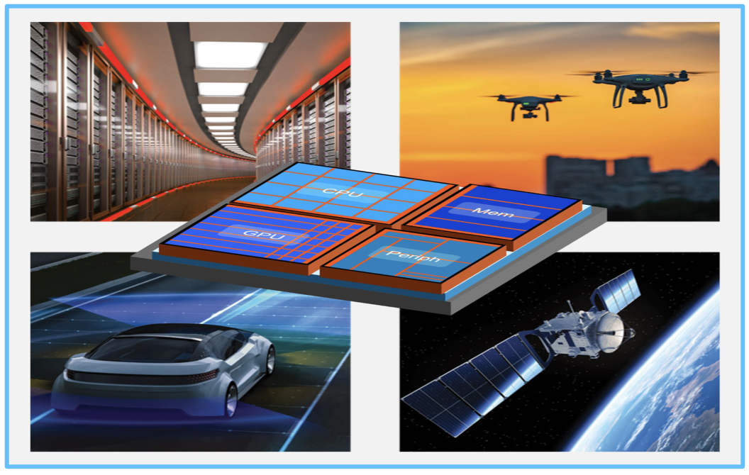
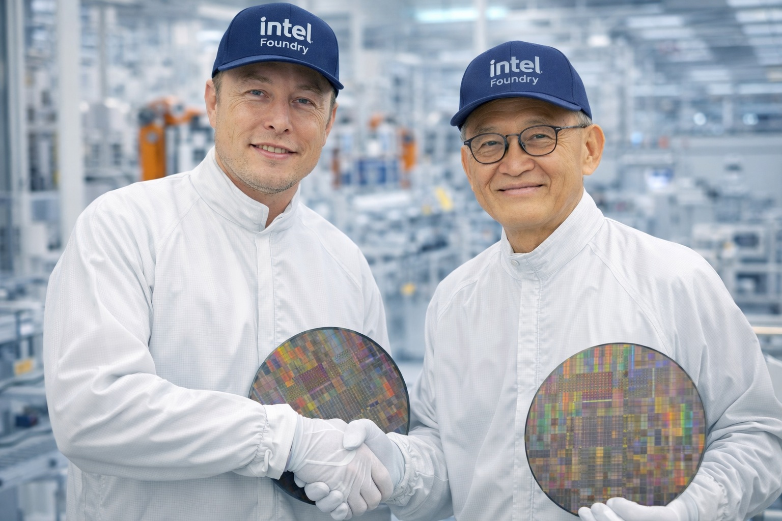


Musk’s Orbital Compute Vision: TERAFAB and the End of the Terrestrial Data Center