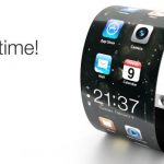
3D TV has been all the rage over the past few years because of the added realism it offers the viewer, but there’s really not that much content that you can stream or play on a Blu-ray device. Wouldn’t it be cool if there was a box that could create 3D on the fly from a 2D stream or Blu-ray? This week I discovered that such a box… Read More
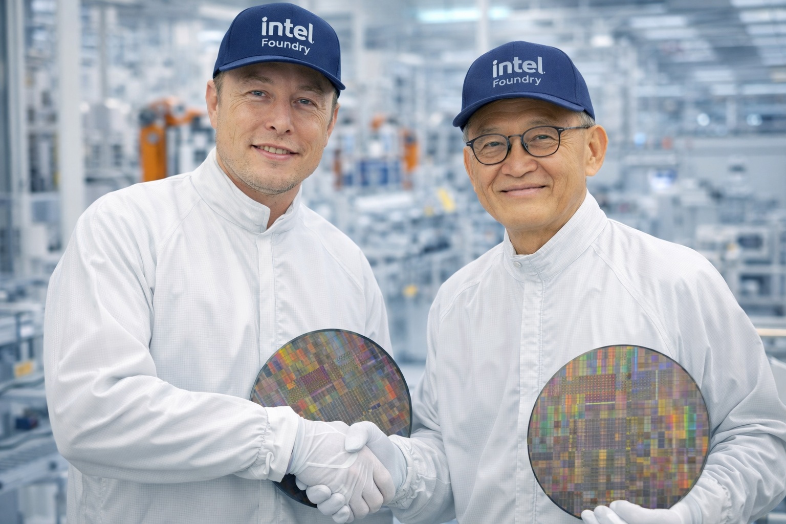 Captain America: Can Elon Musk Save America's Chip Manufacturing Industry?Intel has posted three consecutive years of falling…Read More
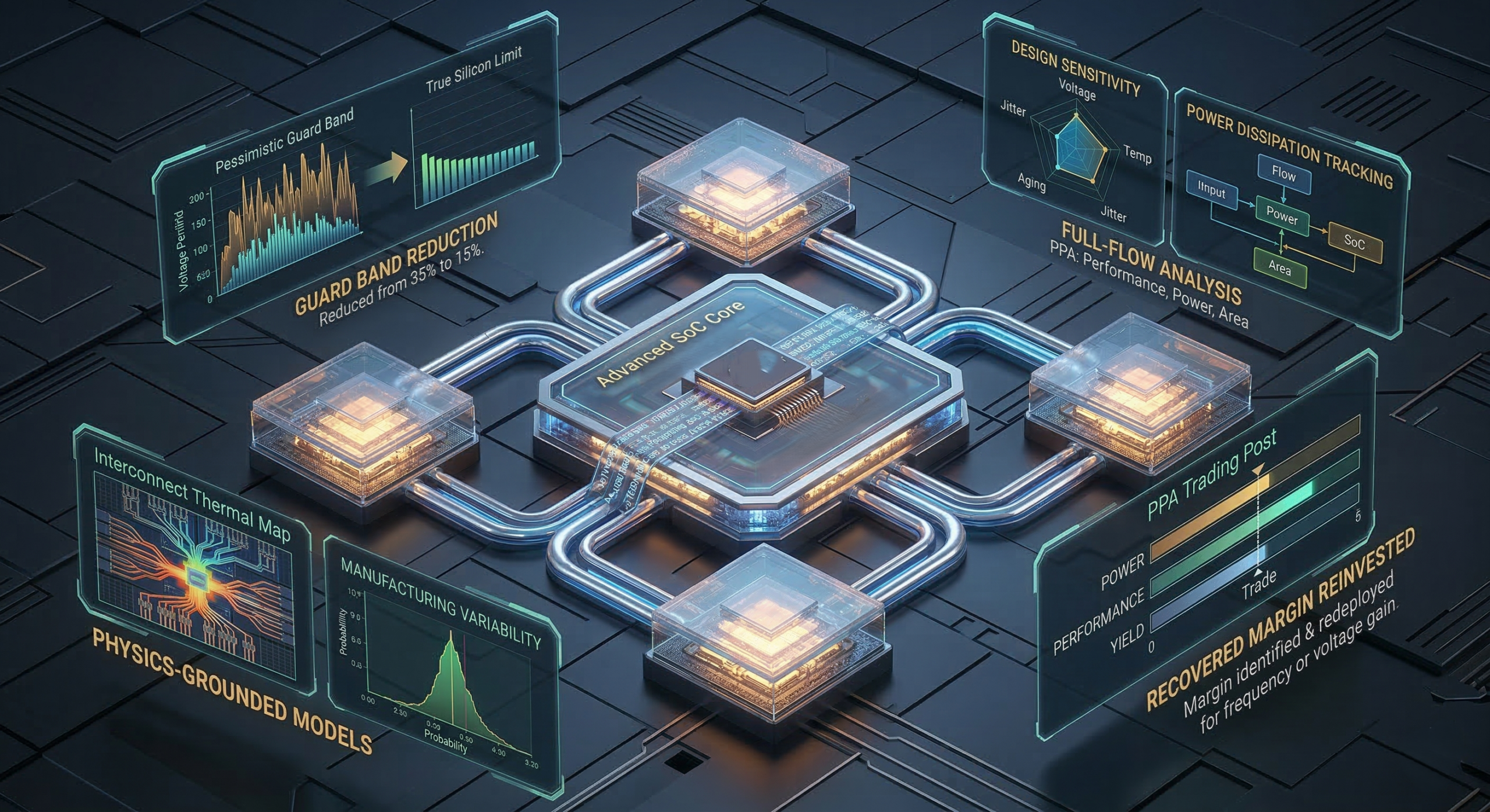 WEBINAR: Reclaiming Clock Margin at 3nm and BelowAt 3nm and below, clock networks have quietly…Read More
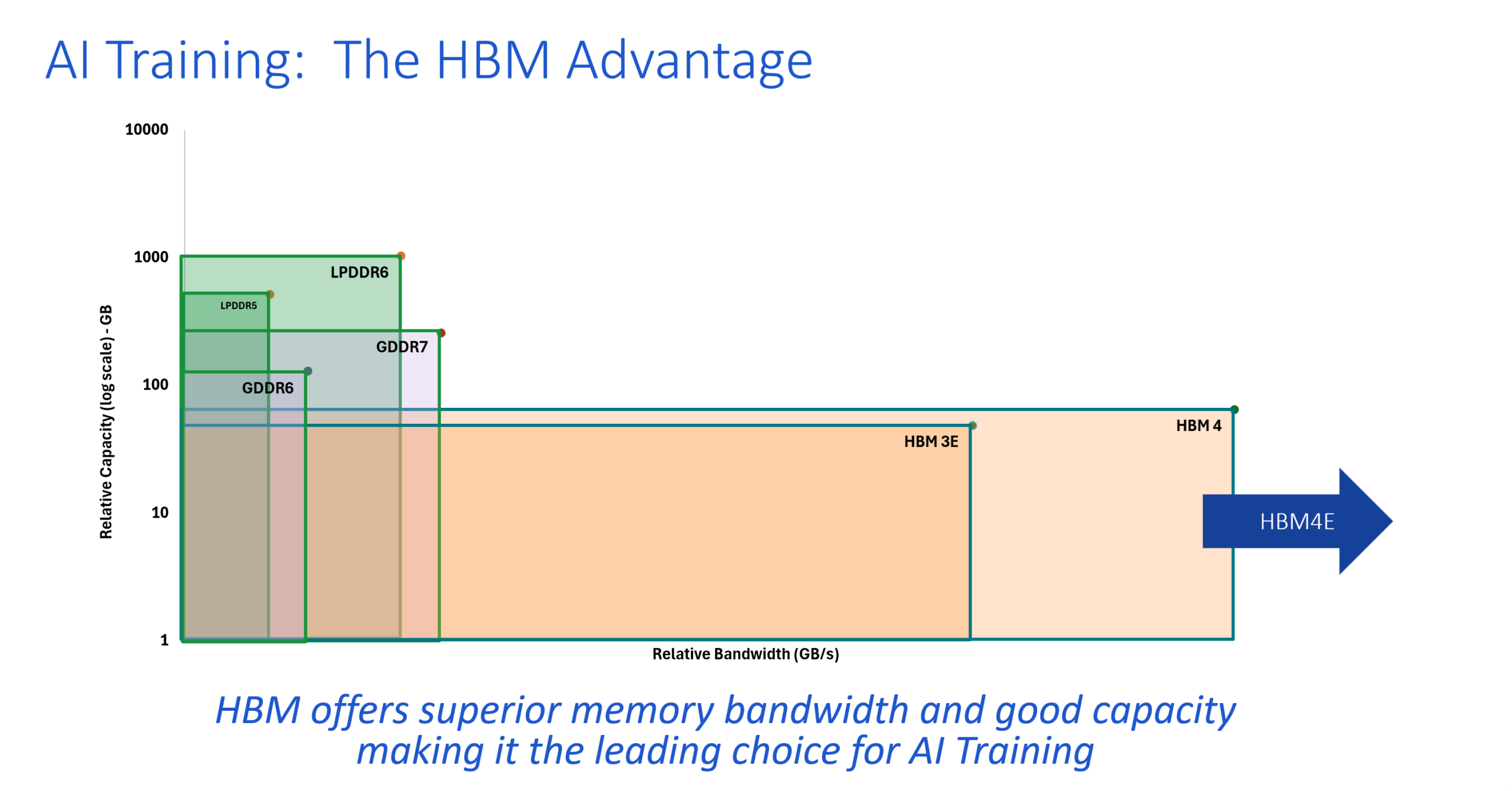 WEBINAR: HBM4E Advances Bandwidth Performance for AI TrainingThe rapid proliferation of LLMs and other AI…Read More
 Siemens Wins Best in Show Award at Chiplet Summit and Targets Broad 3D IC Design EnablementThe recent Chiplet Summit in Santa Clara was…Read More
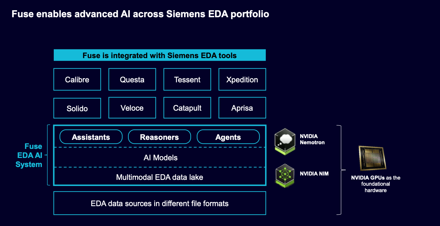 Siemens Fuse EDA AI Agent Releases to Orchestrate Agentic Semiconductor and PCB DesignThough terminology sometimes get fuzzy, consensus holds that…Read More
Jasper at DVCon and EJUG
The Jasper European User Group meeting (EJUG) is coming up in a couple of weeks. It will be held in the Munich Hilton (which I have stayed in many times, the S-bahn from the airport pretty much stops in the basement) on April 2nd.
The schedule for the day is:
9:00 AM – Registration and continental breakfast
9:30 AM – Jasper… Read More
Cadence and ARM BFF

The biggest market for semiconductors is mobile and an ARM processor is the center of the axle around which it revolves. So everyone in the mobile ecosystem needs to work closely with ARM. At CDNLive earlier this week Cadence and ARM announced that they are deepening their partnership. Most of what they announced makes it a lot easier… Read More
Designing for Wearables!
Wearables are going to be a real game changer for the fabless semiconductor ecosystem, absolutely. What other high volume semiconductor market segment has such a low barrier of entry? Speaking of low barrier of entry, the first stop on my Southern California trip last week was Monrovia, the home of Tanner EDA. Tanner is already … Read More
Galileo, not a barber, but an Intel maker module
Words often have much deeper meaning than first meets the ear. The story behind a lyric, or a name, reveals origins, philosophical themes, and ideas beyond the obvious. A new effort from Intel conjures up just such an example – a deep reference to makers everywhere.
In a familiar refrain from Queen “Bohemian Rhapsody,” we hear two… Read More
Mark your Date for Semiconductor Design Vision
A very popular acronym is ‘WYSIWYG’ – What You See Is What You Get! This is very true and is important to visualize things to make it better in various aspects such as aesthetics, compactness, organization, structure, understandable for correction and so on; the most important, in case of semiconductor design, is being able to identify… Read More
A Tool Conceived With Designers’ Input and Developed from Scratch
If we look at the past, most of the EDA tools in the semiconductor design space have originated from a designers’ need to do things faster. Regardless of whether it is design exploration, manual design, simulation, verification, optimization (Power Performance Area – PPA) and many other steps in the overall design flow.… Read More
Now even I can spot bad UVM
Most programmers can read a code snippet and spot errors, given enough hours in the day, sufficient caffeine, and the right lens prescription. As lines of code run rampant, with more unfamiliar third-party code in the mix, interprocedural and data flow issues become more important – and harder to spot.
Verification IP particularly… Read More
DSP running 10 times faster at ultra-low voltage?
The LETI and STMicro have demonstrated a DSP that can hit 500 MHz while pulling just 460mV – that’s ten times better than anything the industry’s seen so far. Implemented on a 28nm FD-SOI technology, with ultra thin forward body biasing (UTFBB) capability (used to decrease Vth), this DSP can also be exercised at higher voltage when… Read More
The Infamous Intel FPGA Slide!
As I have mentioned before, I’m part of the Coleman Research Group so you can rent me by the hour to better understand the semiconductor industry. Most of the conversations are by phone but sometimes I do travel to the East Coast, Taiwan, Hong Kong, and China for face-to-face meetings. Generally the calls are the result of an event … Read More
Chemical Origins of Environmental Modifications to MOR Lithographic Chemistry