Process shrinks, which have served us well for most of the Moore’s Law journey, are reaching their limits. For switching transistors, the biggest problems of leakage current and gate oxide vulnerability in planar MOSFETs have led the industry to new 3D microstructures such as FinFET. For non-volatile memory, the problem is generally… Read More
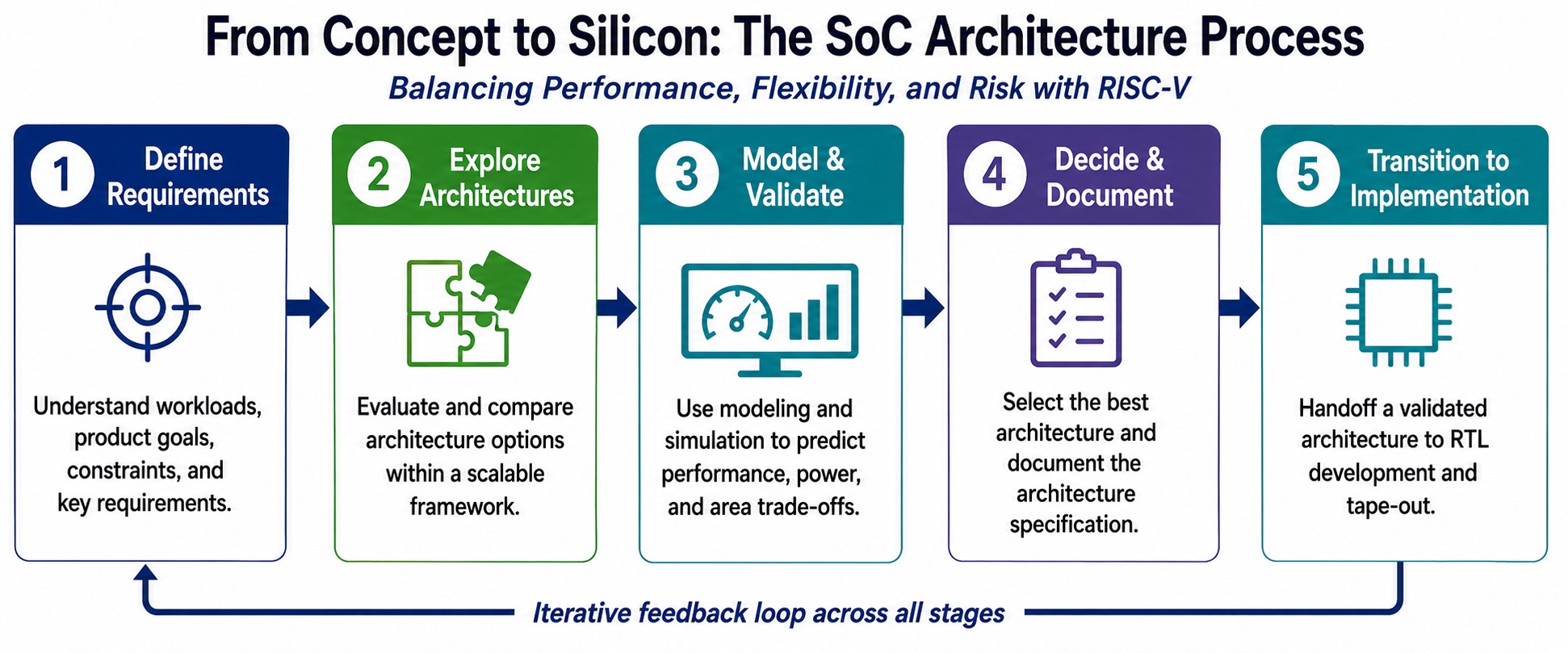 AION Silicon: Architecting Smarter SoCs with RISC-V: Balancing Performance, Flexibility, and Risk Architecting Smarter SoCs with…Read More
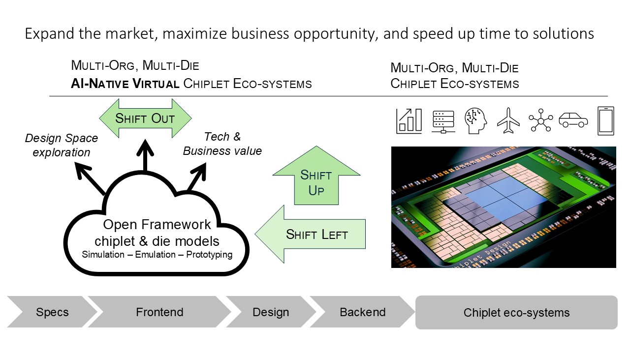 AI-native Virtual Chiplet Eco-systems: Shift Left, Shift Up, and Shift Out to accelerate Chiplet adoptionSystems-in-package (SIPs) with 2.5D and 3D heterogenous integration,…Read More
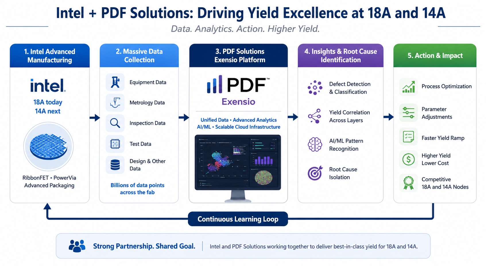 The Yield Partnership: Intel and PDF Solutions Tackle Advanced NodesOne of the most difficult things to do…Read More
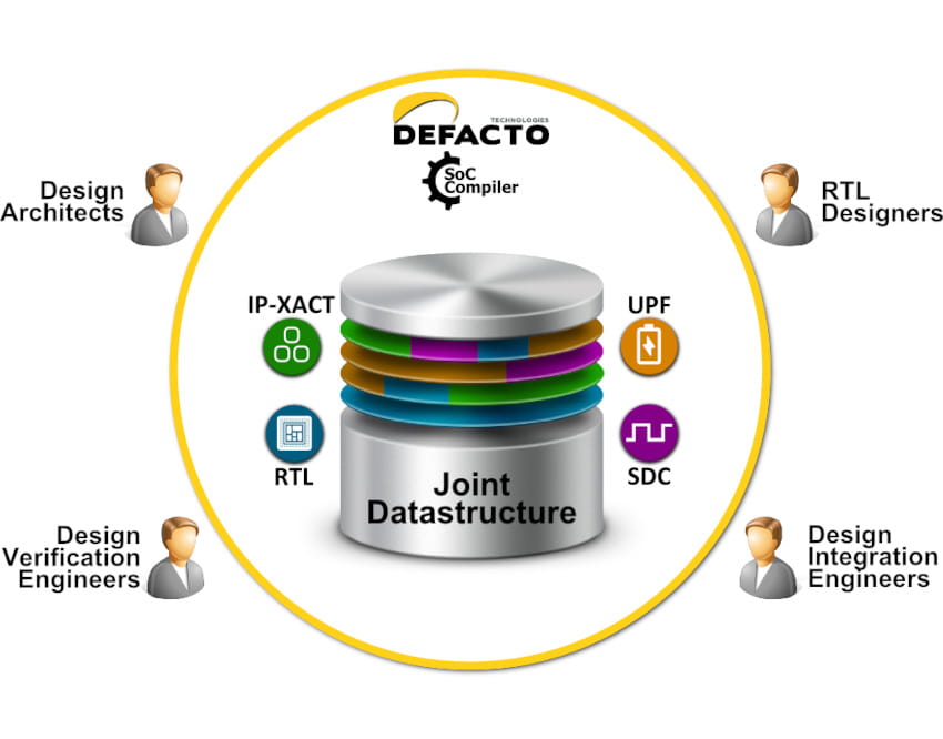 Webinar: Faster Design Spec to Implementation using IP-XACTAs SoC design flows grow increasingly complex, IP-XACT…Read More
 Webinar: Caspia Shows You How to Fix Security Flaws Before It’s Too LateI recently posted an overview of an upcoming…Read More
Expert Tool to View and Debug Design Issues at Spice Level
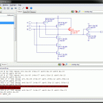
Spice view of a design, block or fragment of the design is probably the lowest level of functional description of a circuit in terms of transistors, resistors, capacitors, interconnect and so on, which in several ways acts as an ultimate proof of pudding for any semiconductor design before manufacturing. However, it’s generally… Read More
Transceiver Verification of a 20nm Altera FPGA Device
FPGA devices are a great way to drive silicon technology development because they contain both digital and analog IP, along with sophisticated IO cells. The highest performance IOs are transceivers, and Altera has recently designed the Arria 10 device family to include up to 96 transceivers, using a 20nm technology that can achieve… Read More
Humans Need Not Apply!
With four children entering the job market I have a very simple piece of advice: DO NOT RUN FROM TECHNOLOGY, EMBRACE IT! Smartphones are now a “natural” part of modern life. We work on them, we play on them, we shop with them, we socialize with them, even risk our lives using them. Come on, every single person with a smartphone has used… Read More
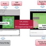
Smart Collaborative Design Reduces Business Risk

The semiconductor design industry is ever challenged with increasing chip density, manufacturing complexity with cutting-edge technologies, accommodating multiple IPs with different functionalities from various sources, optimizing power, performance and cost, maximizing manufacturability and reliability and still… Read More
What’s eSilicon Up To Now?
eSilicon, in conjunction with King Research, is conducting an unusual survey. A lot of vendor-driven surveys focus on specific pain points that are addressed by that particular vendor’s product/service. The idea is typically to either promote visibility for the product/service or establish its undeniable need in the market.… Read More
What Apple Talked About on 9/9/2014
In America the popular press talks almost non-stop about: Disasters, politicians, celebrities and Apple. Yes, Apple. Today I watched the live cast of the new Apple product announcements.
iPhone 6
First, the see things differently video started playing, then the live stream died so I had to turn over to CNET where they were live … Read More
Intel CEO Misinformed on the Foundry Business
At the Citi Global Technology Conference last week Intel (INTC) CEO Brian Krzanich made some comments about the foundry business that I found quite misinformed. It will be interesting to see if this theme is repeated during the foundry presentations at the Intel Developer Forum in San Francisco this week:
Intel is presenting two… Read More
A Comprehensive Power Analysis Solution for SoC+Package
Since power has become a critical factor in semiconductor chip design, the stress is towards decreasing supply voltage to reduce power consumption. However, the threshold voltage to switch devices cannot go down beyond a certain limit and these results in an extremely narrow margin for noise between the two. And that gets further… Read More
What Does Intel Look Like 10 Years From Now?
Intel (INTC) CEO Brian Krzanich keynoted the Citi Global Technology Conference last week. This was a precursor to the Intel Developer Forum in San Francisco this week. Normally these types of events are scripted dog and pony shows but sometimes interesting information comes out. The first question for example:
What does Intel… Read More
Intel 18A vs Intel 18A-P: What Is the Difference and Why Does It Matter?