I visited AtrentaNoida in August 2013 during the inauguration of its newly expanded facility. At that time, I had written about the beautiful environment Atrenta has, with its presence at many sites across the world in my blog – “Innovation + Thoughtful Management = Productive Expansion”. Innovation cannot happen without happy… Read More
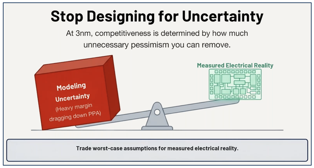 Webinar – How to Reclaim Margin in Advanced NodesThis informative webinar discusses a significant issue that…Read More
 Alchip’s Leadership in ASIC Innovation: Advancing Toward 2nm Semiconductor TechnologyAlchip Technologies has recently reported significant progress in…Read More
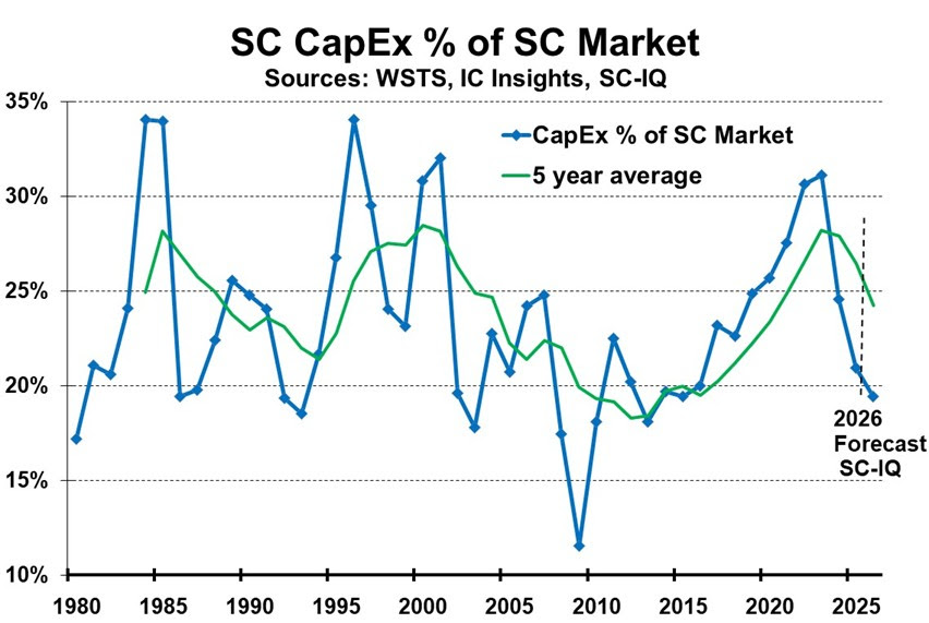 CapEx Up for Foundry, MemorySemiconductor Intelligence estimates total semiconductor industry capital spending…Read More
 RISC-V Now! — Where Specification Meets Scale!In forty plus years as a semiconductor professional…Read More
Twelve Years of Sonics at Toshiba
Sonics announced today that Toshiba has completed the SoC design using Sonics’ on-chip network IP for its new TZ2100 group of application processors. The TZ2100 group of applications processors are the newest addition to Toshiba’s ApP Lite (Application Processor Lite) TZ2000 series. With this group of ApP Lite devices, sound… Read More
Semiconductor Design: Chips to Systems!
This is the 20[SUP]th[/SUP] year of DesignCon and I’m really looking forward to it. While I haven’t attended all 20 I certainly have attended the majority of them. Now it is like a college reunion for me seeing all sorts of friends and former coworkers. One of them is even a keynote but more on that later. This year there are 14 conference… Read More
Je Suis Charlie
Last Monday was the first working day of 2015, dedicated to installing a new PC. Tuesday was also dedicated to an admin work, asking for a new passport, so Wednesday was supposed to be the first real working day for me. In fact, because the Radio is on when I am working, I heard about this crazy offense against the complete editorial board… Read More
Intel’s Diversity Goals Explained!
One of the more interesting announcements by Intel at CES was surprisingly not about technology, it was about a $300M Investing in Diversity and Inclusion initiative. According to Intel CEO Brian Krzanich “A fully diverse and inclusive workplace is fundamental to our ability to innovate and deliver business results.” After … Read More
Wanna Buy a Used Stepper? Only One Owner, Mint Condition…
Back in the early 90s there used to be a billboard alongside 237 advertising second-hand fab equipment: steppers, ion implanters, diffusion ovens. It used to amuse me as an “only in silicon valley” thing; after all, even in silicon valley the number of individuals who were likely to be in a position to buy used fab equipment… Read More
Curie to Bring New Dimensions in Wearables!
In the past year, seeing the kinds of wearables doing what Smartphones can do, I wasn’t much excited about wearables; however after looking at what Intelhas demonstrated in CES 2015, a button sized SoC called Curie, I get to believe that it will be a game changer in wearables and would let Intel do what it couldn’t do with Smartphone… Read More
Mentor Moves to Enter IoT Fray
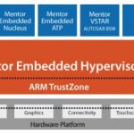
In December I signed up for an IoT “lunch and learn” hosted by Mentor Graphics. There were a number of surprising things about the session. The first and most obvious is that it was really a “breakfast-to-lunch and learn”. Starting at 9AM and going through the end of lunch, it was packed full of ‘learning.’ It was also packed full of … Read More
Makers get access to Intel RealSense
One of the great devices in maker lore is the Polaroid 6500 Series Sonar Ranging Module. It was originally part of the autofocus system for their SX-70 cameras circa 1978, long before through-the-lens optical autofocus sensors were perfected. Back then, people couldn’t focus. Dr. Land thought he was teaching people to compose… Read More
Tizen to connect Samsung’s world – Can it set new equations?
The USA has very good culture of demonstrating new innovations in every industry by way of conferences, exhibitions, workshops, large meetings and so on. The Consumer Electronic Show (CES) is one of its kinds which exhibit new electronic products that tell about which way the industry is heading. Electronic products are final… Read More
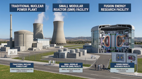
Musk’s Orbital Compute Vision: TERAFAB and the End of the Terrestrial Data Center