You are currently viewing SemiWiki as a guest which gives you limited access to the site. To view blog comments and experience other SemiWiki features you must be a registered member. Registration is fast, simple, and absolutely free so please,
join our community today!
Digital verification engineers have developed robust, thorough metrics for evaluating design coverage. Numerous tools are available to evaluate testbenches against RTL model descriptions — e.g., confirming that simulation regressions exhaustively exercise signal toggles, RTL statement lines, individual statement… Read More
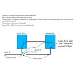
I want to compliment ChipGuy on a very nice write-up of a complex topic – how to model process variation in static timing.
… Read More
In our previous post on SoC memory resource planning, we shared 4 goals for a solution: optimize utilization and QoS, balance traffic across consumers and channels, eliminate performance loss from ordering dependencies, and analyze and understand tradeoffs. Let’s look at details on how Sonics is achieving this.… Read More
IoT Big Data Aggregation
US20140297826 illustrates a system for big data aggregation in a sensor network. The most important part of the Internet of Things (IoT) big data analytics is collecting data before storing the data. The Hadoop big data platform supports collecting data in Hadoop Distributed File System (HDFS). HDFS … Read More
The prevailing industry trends are clear: (1) PCB and die package designs are becoming more complex, across both mobile and high-performance applications; (2) communication interface performance between chips (and their related protocols) is increasingly demanding to verify; (3) signal integrity and power integrity issues… Read More
CMOS Radio Frequency Image Sensor Processby Students@olemiss.edu on 04-03-2016 at 4:00 pmCategories: EDA
Image censoring with radio frequency (RF) in CMOS is a combination of light sensing chips and wireless communication. Typically, we were first engaged in the article, “RF Design Issues and Challenges in a CMOS Image Sensor Process”, because of the circuit design process required to make a functioning Radio Frequency transceiver.… Read More
With the coming onslaught of IoT designs from big companies and small, the opportunity for IoT FPGA prototyping deserves a closer look. This session will start off with a keynote “The Internet of Trust and a New Frontier For Exploration” and will be followed by a discussion with industry experts Don Dingee, Frank Schirrmeister,… Read More
I read with interest a recent article in the San Jose Mercury News (Live Video) about how the availability of better quality cameras on smartphones and the growing appetite for on-demand content on social media now have Facebook and Twitter competing head to head to encourage more people to stream raw footage. Pre-recorded videos… Read More
If you’re in the chip biz in Silicon Valley, check out the SOI Consortium FD-SOI Symposium on April 13th in San Jose. They’ve been running these things since 2009, and I have to say that this one is the most comprehensive to date. Headliners include Cisco, Sony, NXP, SigmaDesigns, ARM, Ciena plus the big FD-SOI foundries,… Read More
Make-versus-buy inadequately describes what we do now in electronic systems design. We are on a continuum of design IP acquisition and use decisions, often with a portfolio of active projects and future projects depending on the outcome. Properly managing IP means adopting a build-borrow-buy mindset and tools capable of handling… Read More


Enhancing Multi-Domain System Simulation with FMI Co-Simulation