DesignCon is a unique conference — its tagline is “Where the Chip meets the Board”. Held each January in Santa Clara, the conference showcases a wealth of new technologies for advanced packaging, printed circuit board fabrication, connectors, cables, and related analysis equipment (e.g, BERT, VNA, scopes). Of specific… Read More
 Scaling Multi-Die Connectivity: Automated Routing for High-Speed InterfacesThis article concludes the three-part series examining key…Read More
 Arteris Highlights a Path to Scalable Multi-Die Systems at the Chiplet SummitAt the recent Chiplet Summit, presentations, discussions and…Read More
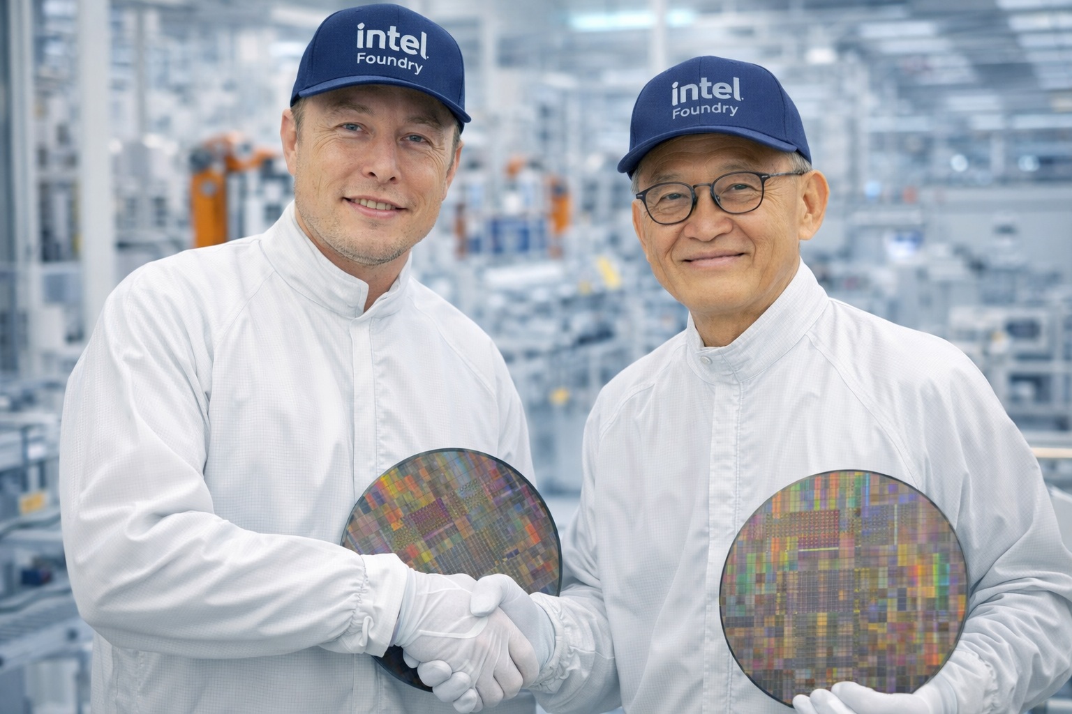
 Captain America: Can Elon Musk Save America's Chip Manufacturing Industry?Intel has posted three consecutive years of falling…Read More
Crypto Key Exchange …like taking candy from a digital baby
For those among you who have read my previous SemiWiki articles, you will no doubt see a theme: the security of our connected world is badly broken, and for the bad guys, violating our online lives – both business and personal – is as easy as taking candy from the proverbial baby.… Read More
The Mechanical Reliability of IC Packages
At Intel back in the late 1970’s we were designing DRAM chips and mounting them in ceramic and plastic packages, however there were problems when some of the die would crack inside of the package because of thermal mismatch issues with how the die was attached to the heat spreader inside the package. Back then we really didn’t… Read More
5nm Chips? Yes, but When?
For any invention, technical proof of concept or prototyping happens years ahead of the invention being infused into actual products. When we talk about 5nm chip manufacturing, a test chip was already prototyped in last October, thanks to Cadence and Imec. Details about this chip can be found in a blog at Semiwiki (link is given … Read More
2016 Samsung Foundry Update!
When sketching out the chapters for our book “Mobile UnLeashed” we sought out the events and technology that empowered the mobile devices that literally changed our world. One of the companies that enabled this change of course is Samsung. Cleverly embedded in chapter 8 “To Seoul, via Austin” is the story of how Samsung got into … Read More
Domain Crossing Verification Needs Continue to Grow
Clock domain crossing (CDC) analysis has been around for many years, initially as special checks in verification or static timing analysis, but it fairly quickly diverged into specialized tools focused just on this problem. CDC checks are important because (a) you can lose data or even lock up at, or downstream of a poorly-handled… Read More
Evaluating the Performance of Design Data Management Software
In the wake of increased global competitiveness and shorter time-to-market windows, there has been a renewed focus by design management on the underlying data management infrastructure of the design teams. An increasing number of systems-on-chip (SoCs) now have some type of analog, digital and/or RF modules, making it imperative… Read More
New Vision for Traffic Cameras in 2016
A picture may be worth a thousand words, but a traffic camera video may be worth millions. TrafficLand is poised to transform forever the use of traffic camera video information with demonstrations at the CES show in Las Vegas. In the process, TrafficLand will be overcoming years of industry ambivalence toward the use of traffic… Read More
IoT in Action : Snowy Smart Cities
I have a gorgeous view outside my home. Everything is covered under more than 2 feet of snow. My flight for tomorrow is cancelled and schools are shut down until Tuesday. For my children, its probably a dream come true but for businesses, it doesn’t help when things come to a standstill. Also for many who need to be on the road, … Read More
The Fine Art of Engineering
There’s a small art gallery near the office. It features a new set of paintings by a local artist every two weeks. As I walk by I tend to check out what’s hanging in there. Sometimes I turn up my nose at what I see – a bit too wacky, a bit too abstract, a bit too paint by numbers. Sometimes I walk in to take a closer look but leave the shop empty-handed… Read More


Silicon Insurance: Why eFPGA is Cheaper Than a Respin — and Why It Matters in the Intel 18A Era