
We’ve heard recently from several sources that millimeter wave radios, once the exclusive realm of defense and satellite use, are now finding homes in applications such as automotive radar and 5G networks. Therein lies a significant opportunity for digital design: moving frequency conversion and filtering from the analog … Read More
 Post-Silicon Validating an MMU. Innovation in VerificationSome post-silicon bugs are unavoidable, but we’re getting…Read More
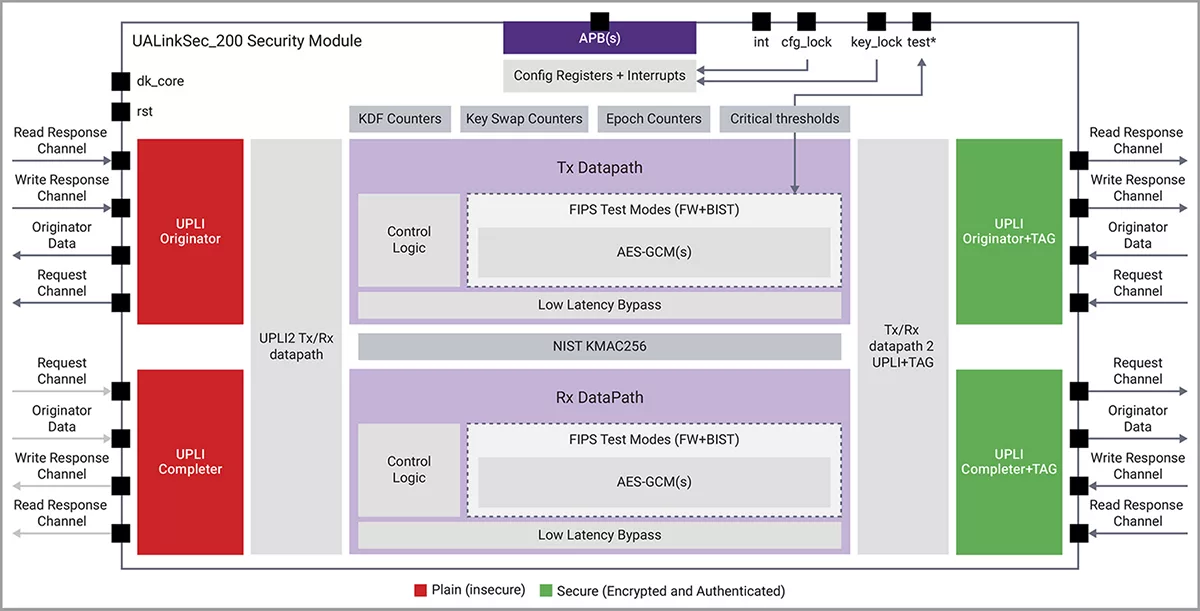 Securing UALink in AI clusters with UALinkSec-compliant IPA classic networking problem is securing connections with…Read More
 GTC 2026: Agentic AI for Semiconductor Design and Manufacturing Janhavi Giri, PhD Principal…Read More
 Scaling Multi-Die Connectivity: Automated Routing for High-Speed InterfacesThis article concludes the three-part series examining key…Read More
At What Point Does Transistor Gate Length Stop Getting Smaller?
When I started doing IC design back in 1978 we had 6,000 nm channel gate lengths, and today you can buy a smart phone with 16 nm or 14 nm technology, although the gate lengths in those phones are more like 34 nm. The International Technology Roadmap for Semiconductors (ITRS) makes predictions about emerging trends in our industry and… Read More
A Credible Player at the Power Table

For a while it seemed like Mentor lived on the margins of the (RTL) design-for-power game. They had interesting micro-architectural optimization capabilities through their Calypto heritage but no real industry chops in power estimation, a must-have when you are claiming to reduce power. Better known offerings in RTL power … Read More
efabless: Think GitHub for ICs and IP
For those of you who don’t know, GitHub is the crowdsourcing version of the defacto industry standard GIT source code management software. Currently, more than 14 million people have deposited more than 35 million software projects (mostly open-source) on GitHub making it the largest host of source code in the world.
Now think… Read More
SEMICON West – Harry Levinson and Mike Lercel Interview
On Tuesday morning at SEMICON I had the opportunity to sit down with Harry Levinson, Sr. Director of Technology Research and Sr. Fellow at Global Foundries and Michael Lercel, Director of Strategic Marketing at ASML to discuss the state of lithography.
I opened the discussion with a question about how we are going to address lithography… Read More
1-T SRAMs in high-density, portable applications
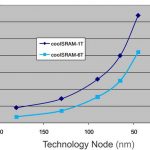
For SoCs designed for various applications such as mobile, automotive, wearable computing, gaming, virtual reality, PC, imaging, security, and IOT applications, it is incredibly important to keep area (cost) and power as low as possible. Considering the growing percentage of chip area used for memory, it makes sense to choose… Read More
Filling out the rest of the mobile device
We spend an inordinate amount of energy tracking the big chip – the application processor – in a mobile device. As we’ve seen this space is coming down to a handful of players. A more interesting competition is heating up around the APU for the rest of chips needed to make a phone.… Read More
Foundry Technology Packaging Solutions
A significant shift is underway in the fabless semiconductor business model. As the application markets have become more diverse (and more cost-sensitive), product requirements have necessitated a new focus on multi-die packaging technology. … Read More
Limits to Deep Reasoning in Vision
If you are a regular reader, you’ll know I like to explore the boundaries of technology. Readers I respect sometimes interpret this as a laughable attempt to oppose the inevitable march of progress, but that is not my purpose. In understanding the limits of a particular technology, it is possible to envision what properties a successor… Read More
AMD Unveils Full Radeon RX 400 Models And Positioning At E3
At E3 2016 in Los Angeles, California Advanced Micro Devices disclosed the numbering and targeted use cases of their full line of Polaris-based GPUs, branded as the “Radeon RX Series” of graphics cards. Advanced Micro Devices had previously disclosed some details about the new Radeon RX series of graphics cards at Computex 2016… Read More
Silicon Insurance: Why eFPGA is Cheaper Than a Respin — and Why It Matters in the Intel 18A Era