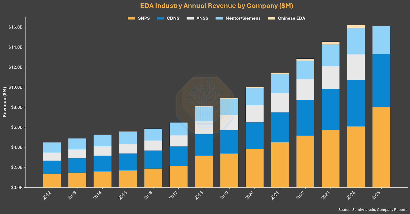
You’re building an IP, subsystem or SoC and you want to use a prototype together with a software testbench to drive extensive validation testing. I’m not talking here about the software running on the IP/SoC processor(s); the testbench should wrap around the whole DUT. This is a very common requirement. The standard approach to… Read More


3D Product Design Collaboration in MCAD and ECAD Platforms
Consumer electronics demand aggressive mechanical enclosure design — product volume, weight, shape, and connector access are all critical design optimization criteria. Mechanical CAD (MCAD) software platforms are used by product engineers to develop the enclosure definition — the integration of the PCB design… Read More
The CDNLive Keynotes
I’m developing a taste for user-group meetings. In my (fairly) recently assumed role as a member of the media, I’m only allowed into the keynotes, but from what I have seen, vendors work hard to make these fresh and compelling each year through big-bang product updates and industry/academic leaders talking about their work in bleeding-edge… Read More
NetSpeed Taking a Ride with Autonomous Automobiles
The push for autonomous automobiles continues at a rapid pace. Last week a new conference was held in Santa Clara, CA by the Linley Group focused on Autonomous Hardware. The group included presentations from GLOBAL FOUNDRIES, Synopsys, NetSpeed Systems, Arteris, EMBC, Cadence, CEVA, ARM and Trilumina covering ADAS and autonomous… Read More
1.2 Terabit/s C2C Interface? Only with Interlaken!
If you are familiar with high bandwidth networking applications, you probably know this chip-to-chip (C2C) interface protocol. Interlaken architecture, fully flexible, configurable and scalable, is also an elegant answer to the need for very high bandwidth C2C communication. Interlaken is elegant because the protocol … Read More
Attending DAC in Austin for Free
I’ve been attending DAC since the late 1980’s and can tell you that it’s an annual highlight for me and anyone else interested in the EDA, IP and semiconductor industries. Where else can you see most of the big and little vendors of EDA software, semiconductor IP and foundries in one place? I recently blogged about… Read More
How Far Has Design Automation Brought Us?
It’s always a struggle explaining electronic design automation (EDA) to people who ask me what field I am in. I have come up with simple and minimal descriptions – such as “software used for designing semiconductors.” This, of course, does little to provide any useful understanding to people who are not familiar with the field.… Read More
Machine Learning and EDA!
Semiconductor design is littered with complex, data-driven challenges where the cost of error is high. Solido’s new ML (machine learning) Labs, based on Solido’s ML technologies developed over the last 12 years, allows semiconductor companies to collaboratively work with Solido in developing new ML-based EDA products.
Data… Read More
The 4C’s of PCB Design
The diamond jewelry industry encourages customers to focus on the 4C’s — cut, clarity, color, and carats. At the recent PCB Forum conducted by Mentor (a Siemens business) in Santa Clara, I learned that current system design flows also require an emphasis on the 4C’s — collaboration, concurrency, consistency… Read More
Webinar: Getting to Formal Coverage
Facing rapidly growing challenges in getting to respectable coverage, designers have been turning more and more to formal verification, not just to plug gaps but increasingly to take over verification of significant components of the testplan. Which is great, but at the end of the day any approach to verification must be measured… Read More
Rapidus, IBM, and the Billion-Dollar Silicon Sovereignty Bet