In the good old days the clock signal looked like a square wave , and had a voltage swing of 5 volts, however with 7nm technology the clock signals can now look more like a sawtooth signal and may not actually reach the full Vdd value of 0.65V inside the core of a chip. I’ll cover some of the semiconductor market trends, and then challenges… Read More
The 5G technology market is huge with incredible growth opportunities for various players within the ecosystem. As a leading cellular IP provider, CEVA has been staying on top of the opportunity by offering solutions that enable customers to bring differentiated products to the marketplace. Earlier this year, SemiWiki posted… Read More
-Micron slams on the brakes of capacity & capex-
-But memory market is already over the cliff without skid marks
-It will likely take at least a year to sop up excess capacity
-Collateral impact on Samsung & others even more important
Micron hitting the brakes after memory market already impacts
Micron capped off an otherwise… Read More
We have written about eFPGA and for six years now and security even longer so it is natural to combine these two very important topics. Last month we covered the partnership between Flex Logix and Intrinsic ID, and the related white paper. Both companies are SemiWiki partners, so we were able to provide more depth and color:
In the … Read More
Listen in on any automotive podcast, earnings call, or attend any automotive industry event and you will hear about “software defined” cars and “service oriented architectures.” This euphemistic terminology obscures the reality that cars in most major markets are almost universally connected – even if the owners of those … Read More
Dan is joined by Scott Almassy, a Partner in PwC’s Trust Solutions business, as well as PwC’s Semiconductor and Infrastructure Lead. In his almost 20 years in the professional services industry, Scott has provided audit and advisory services to semiconductor companies across the industry ranging from the largest… Read More
Author: Paul McWilliams
Dr. Gordon Moore was the Director of Research and Development at Fairchild when he wrote the paper, “Cramming More Components onto Integrated Circuits” that was published in the April 19, 1965 issue of Electronics. Following this publication, Dr. Carver Mead of Caltech declared Dr. Moore’s… Read More
Coby Hanoch comes to Weebit Nano with 15 years’ experience in engineering and engineering management and 26 years’ experience in sales management and executive roles. Coby was Vice President Worldwide Sales at Verisity where he was part of the founding team and grew the company to over $100M in annual sales which facilitated its… Read More
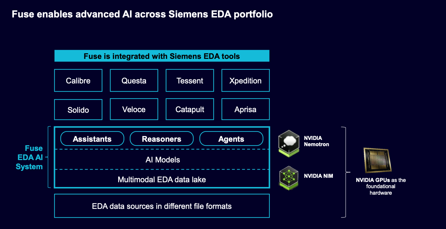
My IC design career started out with manually sizing transistors to improve performance, while minimizing layout area and power consumption. Fortunately we don’t have to do manual transistor sizing anymore, thanks to EDA tools that are quicker and more accurate than manual methods. MunEDA is an EDA vendor that has developed… Read More
New EDA product launches are always an exciting time, and I could hear the energy and optimism from the voice of Manoj Chacko at Synopsys in our Zoom call about Synopsys PrimeClosure. During the physical implementation phase for IC designs there’s a big challenge to reach timing closure, and with advanced nodes the number… Read More


Captain America: Can Elon Musk Save America’s Chip Manufacturing Industry?