Dan is joined by Nigel Drego, the CTO and Co-founder at Quadric. Nigel brings extensive experience in software and hardware design to his role at Quadric. Nigel is an expert in computer architectures, compiler technology, and software frameworks.
Dan explores the unique and unified HW/SW architecture developed by Quadric with… Read More
Mobiveil Marks 11th Anniversary
Ravi Thummarukudy is Mobiveil’s Chief Executive Officer and a founder. He and I recently spent an enjoyable afternoon getting acquainted as I learned more about Mobiveil. It’s an inspiring story of a technology company in the semiconductor space helping customers and prospering.
Eleven-year-old… Read More
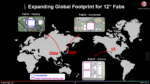
TSMC also covered manufacturing excellence. The TSMC “Trusted Foundry” tagline has many aspects to it, but manufacturing is a critical one. TSMC is the foundry capacity leader but there is a lot more to manufacturing as you will read here. Which brings us to the manufacturing accomplishments from the briefing:
To
…
Read More
TSMC covered their specialty technologies in great detail. Specialty is what we inside the ecosystem used to call weird stuff meaning non-mainstream and fairly difficult to do on leading edge processes. Specialty technologies will play an even more important part of semiconductor design with the advent of chiplets where die… Read More
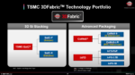
TSMC’s 3DFabric initiative was a big focus at the symposium, as it should be. I remember when TSMC first went public with CoWos the semiconductor ecosystem, including yours truly, let out a collective sigh wondering why TSMC is venturing into the comparatively low margin world of packaging. Now we know why and it is absolutely… Read More
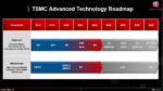
The next topic I would like to cover is an update to the TSMC process node roadmap starting with N3. As predicted, N3 will be the most successful node in the TSMC FinFET family. The first version of N3 went into production at the end of last year (Apple) and will roll out with other customers in 2023. There is a reported record amount of … Read More
The TSMC 2023 North America Technology Symposium happened today so I wanted to start writing about it as there is a lot to cover. I will do summaries and other bloggers will do more in-depth coverage on the technology side in the coming weeks. Having worked in the fabless semiconductor ecosystem the majority of my 40 year semiconductor… Read More
Dan is joined by Charlie Cheng, Managing Director of Polyhedron. Prior to that, Charlie was the CEO of Kilopass Technology, where he grew the core memory business into a successful acquisition by Synopsys. Before that, Charlie was an Entrepreneur in Residence at US Venture Partners and a Corporate VP at Faraday Technology, a Taiwanese… Read More
Artificial Intelligence (AI) is a rapidly growing field that has the potential to revolutionize the way we work, learn, and interact with technology. The term AI refers to the ability of machines to perform tasks that would typically require human intelligence, such as decision-making, problem-solving, and natural language… Read More
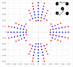
The “1.xnm” node on most roadmaps to indicate a 16-18 nm metal line pitch [1]. The center-to-center spacing may be expected to be as low as 22-26 nm (sqrt(2) times line pitch). The EXE series of EUV (13.5 nm wavelength) lithography systems from ASML feature a 0.55 “High” NA (numerical aperture), targeted… Read More

The Packaging PDK Is the Missing Layer for Co-Packaged Optics