I had the opportunity to preview an upcoming webinar on SemiWiki that deals with design robustness for signoff regarding advanced node digital designs (think single-digit nanometers). “Design robustness” is a key term – it refers to high quality, high yielding SoCs that come up quickly and reliably in the target system. We all… Read More
 WEBINAR: Functional ECO Solution for Mixed-Signal ASIC DesignThis webinar, in partnership with Easy-Logic Technology, is…Read More
 Taming Concurrency: A New Era of Debugging Multithreaded CodeAs modern computing systems evolve toward greater parallelism,…Read More
 Perforce Webinar: Can You Trust GenAI for Your Next Chip Design?GenAI is certainly changing the world. Every day…Read More
 A Principled AI Path to Spec-Driven VerificationI have seen a flood of verification announcements…Read More
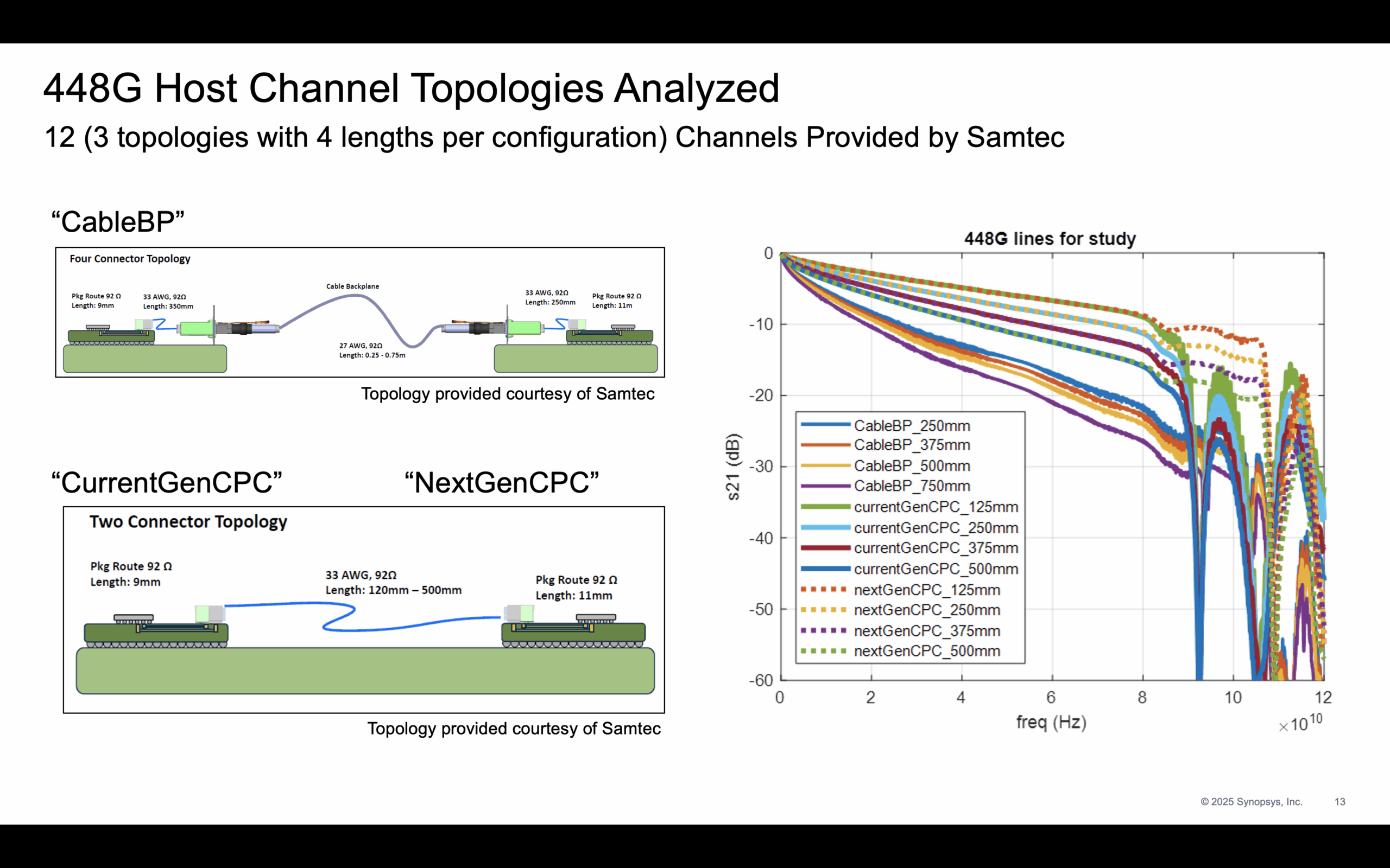
 448G: Ready or not, here it comes!The march toward higher-speed networking continues to be…Read More
Six Automated Steps to Design Partitioning for Multi-FPGA Prototyping Boards
Before starting your next FPGA Prototyping Project you should catch the next SemiWiki webinar – “Six Automated Steps to Design Partitioning for Multi-FPGA Prototyping Boards”, in partnership with Aldec.
A significant portion of my 30+ years in the EDA industry has revolved around design verification with some form of FPGA … Read More
Technology Tyranny and the End of Radio
As technology consumers we make tradeoffs.
We let Google peer into our online activity and email communications and we even accept annoying advertisements tied to our browsing activity in order to access free email and browing. We tolerate smartphones with diminishing performance from Apple – even after Apple admits that the
A Forbidden Pitch Combination at Advanced Lithography Nodes
The current leading edge of advanced lithography nodes (e.g., “7nm” or “1Z nm”) features pitches (center-center distances between lines) in the range of 30-40 nm. Whether EUV (13.5 nm wavelength) or ArF (193 nm wavelength) lithography is used, one thing for certain is that the minimum imaged pitch … Read More
TSMC’s 5nm 0.021um2 SRAM Cell Using EUV and High Mobility Channel with Write Assist at ISSCC2020
Technological leadership has long been key to TSMC’s success and they are following up their leadership development of 5nm with the world’s smallest SRAM cell at 0.021um 2 with circuit design details of their write assist techniques necessary to achieve the full potential of this revolutionary technology. In addition to their… Read More
The Story of Ultra-WideBand – Part 2: The Second Fall
Over-engineered to perfection, outmaneuvered by Wi-Fi
In Part 1 of this series, we recounted the birth of wideband radio at the turn of the 20th century, and how superheterodyne radio killed wideband radios for messaging after 1920. But RADAR kept wideband research alive through World War 2 and the Cold War. Indeed, the story of… Read More
COVID-19 Collateral Chip Collision – Will Fabs & Foundries Flounder?
Corona Fab Impact –
lower production/raise prices
Chip production supply chain may break
It could temporarily fix memory oversupply
Could it risk the fall roll out of next Iphone
The ” Two week tango” – Waiting games at fabs
When a highly specialized piece of semiconductor equipment misbehaves to the… Read More
Designing Next Generation Memory Interfaces: Modeling, Analysis, and Tips
At DesignCon 2020, there was a presentation by Micron, Socionext and Cadence that discussed design challenges and strategies for using the new low-power DDR specification (LPDDR5). As is the case with many presentations at DesignCon, ecosystem collaboration was emphasized. Justin Butterfield (senior engineer at Micron)… Read More
LithoVision – Economics in the 3D Era
Each year on the Sunday before the SPIE Advanced Lithography Conference, Nikon holds their LithoVision event. This year I had the privilege of being invited to speak for the third consecutive year, unfortunately, the event had to be canceled due to concerns over the COVID-19 virus but by the time the event was canceled I had already… Read More
The Story of Ultra-WideBand – Part 1: The Genesis
In the middle of the night of April 14, 1912, the R.M.S. Titanic sent a distress message. It had just hit an iceberg and was sinking. Even though broadcasting an emergency wireless signal is common today, this was cutting edge technology at the turn of the 20th century. This was made possible by the invention of a broadband radio developed… Read More


Should the US Government Invest in Intel?