In High-NA EUV lithography systems, the numerical aperture (NA) is expanded from 0.33 to 0.55. This change has been marketed as allowing multi-patterning on the 0.33 NA EUV systems to be avoided. Only very recently have specific examples of this been provided [1]. In fact, it can be shown that double patterning has been implemented for EUV in cases where DUV double patterning could have sufficed.
What a Higher NA offers
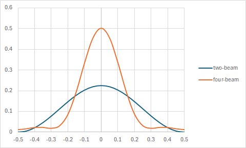
The increase in NA allows more diffraction orders or a wider range of spatial frequencies to be used for imaging. Having more diffraction orders for the same image allows brighter, narrower peaks, as shown in the example of Figure 1.
The sharper peak means the normalized image log slope (NILS) is better, so the stochastic effect of shot noise in the photon absorption won’t be as severe. Consequently, a directly printed image would be more likely to be degraded for 0.33 NA compared to 0.55 NA.
Current EUV Uses Multipatterning
To keep the shot noise low enough to keep the single 0.33 NA exposure, the dose would have to be increased to a point where throughput or resist loss would be a detracting issue, e.g., > 100 mJ/cm2. On the other hand, if the 0.33 NA pattern were split into two separately exposed portions (Figure 2), each one would have a denser range of spatial frequencies due to wider separations between features, which will improve the NILS.
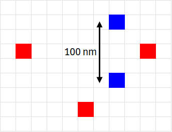
Interestingly, in this case, the minimum 100 nm distance means DUV can also be used with double patterning for the same pattern. This is consistent with an earlier finding that DUV and EUV double patterning may be overlapped due to the impact of stochastic effects [2].
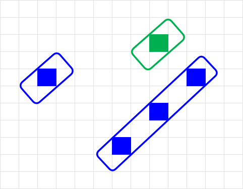
Furthermore, if the pattern of Figure 2 were scaled down by a factor of the NA ratio (0.33/0.55), so that the via size becomes 36 nm x 0.6 = 21.6 nm, the same situation will apply to the High-NA case as well, since the spatial frequency range (normalized to 0.55 NA) is now reduced to the same as previously for 0.33 NA. This means we should expect double patterning for High-NA EUV, triple patterning for low-NA EUV, and quadruple patterning for DUV (Figure 3).

On the other hand, it can be noted that via patterns can conform to a diagonal grid [3], which would enable DUV/low-NA double patterning or High-NA EUV single patterning for location selection if the vias are fully self-aligned (Figure 4).
High-NA Depth of Focus Challenged by Resist Thickness
A fundamental consequence of having a wider range of spatial frequencies in a larger numerical aperture is that there is a wider range of optical paths used in forming the image. Each path corresponds to an angle with the optical axis. At the wafer, the wider range leads to the higher spatial frequencies getting more out of phase with the lower ones, causing the image to lose contrast from defocus. This is visualized in Figure 5.
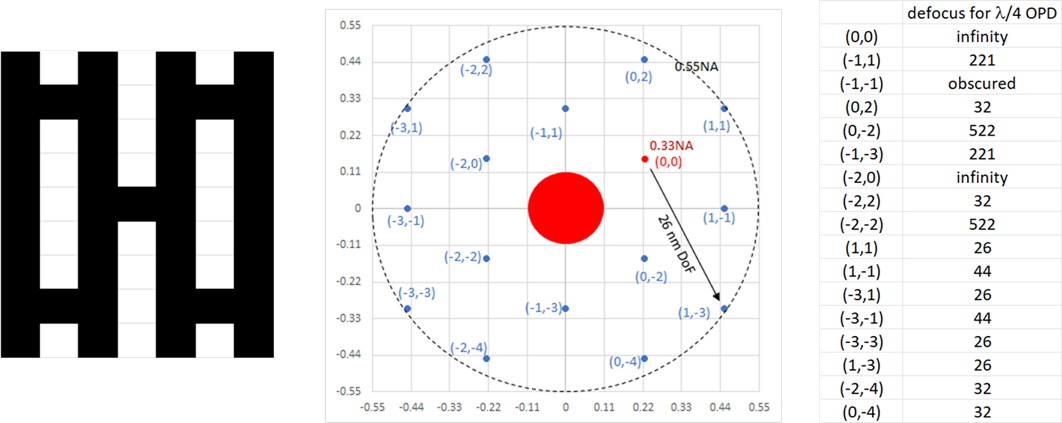
As Figure 5 shows, this is particularly bad for line breaks, where the tip-to-tip distance needs to be controlled. Likewise, it would apply to the corresponding line cut pattern. The depth of focus reduction applies generally to patterns with wide spacings between features such as the random via pattern of Figure 2. Figure 6 shows that even 15 nm defocus is enough to significantly affect a 40 nm pitch line pattern, due to four diffraction orders being included by a 0.55 numerical aperture as opposed to two diffraction orders for a 0.33 numerical aperture.
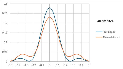
To preserve the image uniformity as much as possible through the resist thickness, the resist thickness needs to be at most as thick as the depth of focus. A depth of focus < 30 nm for High-NA means resist thickness has to be < 30 nm, which may further experience 50% resist thickness loss [4]. Such a thin retained resist layer also would have absorbed very little EUV, leading to even greater absorbed photon shot noise and greater sensitivity to electrons from the underlayer [5] as well as the EUV plasma [6].
Thus, though obviously not mentioned in the marketing, it is reasonable to expect that High-NA EUV exposure cannot provide enough depth of focus for a reasonable resist thickness, and any future Hyper-NA (at least 0.75 [7]) would be even worse.
References
[1] C. Zahlten et al., Proc. SPIE 13424, 134240Z (2025).
[2] F. Chen, Can LELE Multipatterning Help Against EUV Stochastics?.
[3] F. Chen, Routing and Patterning Simplification with a Diagonal Via Grid.
[4] F. Chen, Resist Loss Prohibits Elevated Doses; J. Severi et al., “Chemically amplified resist CDSEM metrology exploration for high NA EUV lithography,” J. Micro/Nanopatterning, Materials, and Metrology 21, 021207 (2022).
[5] H. Im et al., Proc. SPIE 13428, 1342815 (2025).
[6] Y-H. Huang, C-J. Lin, and Y-C. King, Discover Nano 18:22 (2023).
[7] G. Bottiglieri et al., Proc. SPIE 13424, 1342404 (2025).
This article first appeared in Exposing EUV: High-NA Hard Sell: EUV Multipatterning Practices Revealed, Depth of Focus Not Mentioned
Also Read:
Impact of Varying Electron Blur and Yield on Stochastic Fluctuations in EUV Resist
Stitched Multi-Patterning for Minimum Pitch Metal in DRAM Periphery
A Perfect Storm for EUV Lithography
Share this post via:




Musk’s Orbital Compute Vision: TERAFAB and the End of the Terrestrial Data Center