A comprehensive update to the EUV stochastic image model
In extreme ultraviolet (EUV) lithography, photoelectron/secondary electron blur and secondary electron yield are known to drive stochastic fluctuations in the resist [1-3], leading to the formation of random defects and the degradation of pattern fidelity at advanced nodes. For simplicity, blur and electron yield per photon are often taken to be fixed parameters for a given EUV resist film. However, there is no reason to expect this to be true, since the resist is inhomogeneous on the nanoscale [4-6].
I have updated the model I have been using to analyze EUV stochastics with the following:
•Image fading from EUV pole-specific shift is not included (expected to be minor)
•Polarization consideration: assume 50% TE/50% TM for 2-beam image commonly used for EUV lines and spaces [7]
•Poisson statistics is applied to absorbed photons/nm2
•Electron blur fixed at zero at zero distance and match exponential attenuation length at larger distances => exp(-x/attenuation length)
•Electron blur is considered locally varying rather than a fixed number
•Electron (or acid) number per absorbed EUV photon has a minimum and maximum number
•Acid blur still uses Gaussian form (s=5 nm)
A key feature is that electron yield per photon is part of a distribution. This distribution is often modeled as Poissonian but in actuality can deviate from it significantly [8]. The maximum number of electrons is roughly the EUV photon energy (~92 eV) divided by the ionization potential (~10 eV), giving 9. TThe minimum number of electrons can be estimated as 6 from the Auger emission scenario in Figure 1, with one electron assumed lost to the underlayer, giving 5.
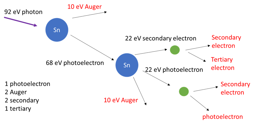
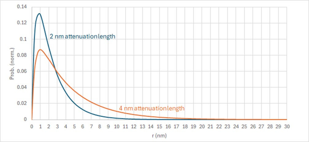
We also recall that electron blur is not a fixed value, but can take on different values at different locations [4-6]. As constructed previously [3], the electron blur function shape arises from the difference of two exponential functions. To maintain zero probability at zero distance, an exponential function with 0.4 nm attenuation length is subtracted from the normalized exponential function with target attenuation length.
While a typical blur can correspond to an attenuation length of ~2 nm, the inhomogeneity within the resist can lead to a rare occurrence of higher blur, e.g., corresponding to an attenuation length of ~4 nm (Figure 2).
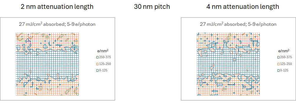
The impact of varying blur is to increase the % of defective pixels in the image (Figure 3). We expect stochastic defectivity to be higher. This is to be expected as increasing blur decreases the max-min difference, making it more likely for particle number fluctuations to cross a given threshold.
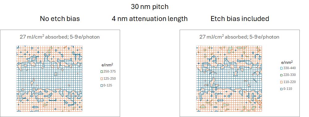
Etching can affect the stochastics in the final image. Etch bias can make obstructions in the trench more likely, or openings between trenches more likely. This is the origin of the “valley” between the stochastic defectivity cliffs (Figure 4).
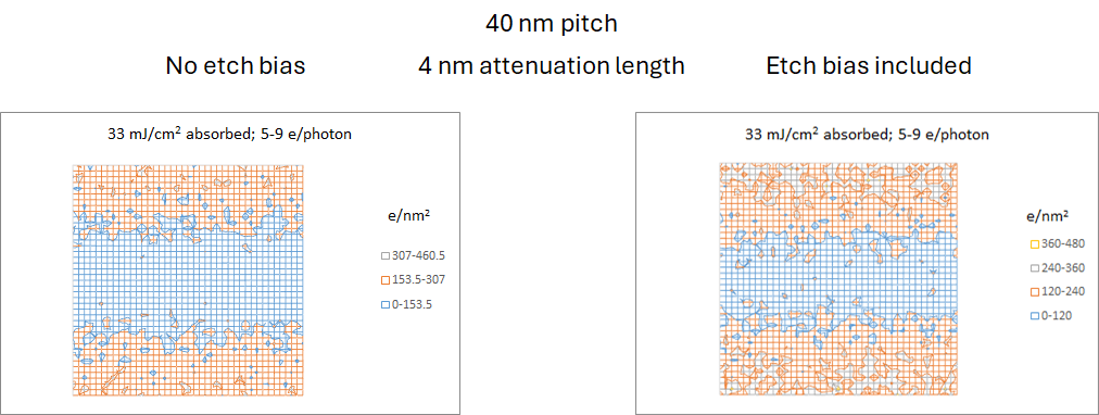
As pitch increases, the contrast loss from the “typical” electron blur shown in Figure 2 will reach a minimum value of 20% [3]. However, the stochastic behavior for larger pitches improves as thicker resists may be used, increasing photon absorption density. Going from 30 nm to 40 nm pitch (Figure 5), the absorbed photon density increases , and the contrast reduction from electron blur is also improved. However, there is still significant noise in the electron density at the edge and defectivity with etch bias.
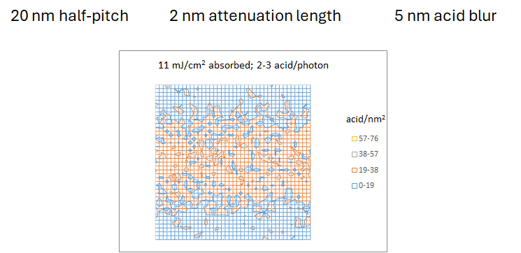
When chemically amplified resists are used, acid blur must be added. Acid blur is usually modeled as a Gaussian function with sigma on the order of 5 nm [9]. The extra blur from acid aggravates the stochastic behavior even more (Figure 6).
Consequently, double or multiple patterning is used with EUV comprising exposures at > 40 nm pitch, with larger features and resist thicknesses. DUV multipatterning will still have the following advantages over EUV multipatterning:
- Polarization restriction (not unpolarized)
- No electron blur
- Higher photon density
- 2-beam imaging (instead of 3- or 4-beam)
- Well-developed phase-shift mask technology
Most importantly, DUV double patterning has lower cost than EUV double patterning.
Thanks for reading Exposing EUV! Subscribe for free to receive new posts and support my work.
References
[1] Z. Belete et al., J. Micro/Nanopattern. Mater. Metrol. 20, 014801 (2021).
[2] F. Chen, A Perfect Storm for EUV Lithography.
[3] F. Chen, A Realistic Electron Blur Function Shape for EUV Resist Modeling.
[4] F. Chen, Measuring Local EUV Resist Blur with Machine Learning.
[5] F. Chen, Stochastic Effects Blur the Resolution Limit of EUV Lithography.
[6] G. Denbeaux et al., “Understanding EUV resist stochastic effects through surface roughness measurements,” IEUVI Resist TWG meeting, February 23, 2020.
[7] H. J. Levinson, Jpn. J. Appl. Phys. 61, SD0803 (2022).
[8] E. F. da Silveira et al., Surf. Sci. 408, 28 (1998); Z. Bay and G. Papp, IEEE Trans. Nucl. Sci. 11, 160 (1964); L. Frank, J. Elec. Microsc. 54, 361 (2005).
[9] H. Fukuda, J. Micro/Nanolith. MEMS MOEMS 19, 024601 (2020).
This article is based on the presentation in the following video: Comprehensive Update to EUV Stochastic Image Model.
Thanks for reading Exposing EUV! Subscribe for free to receive new posts and support my work.


Musk’s Orbital Compute Vision: TERAFAB and the End of the Terrestrial Data Center