
Peak probability at zero distance actually makes no sense
In lithography, it is often stated that the best resolution that can be achieved depends on wavelength and numerical aperture (NA), but this actually only applies to the so-called “aerial” image. When the image is actually formed in the resist layer, it also depends on an additional factor, known as blur.
What blur does is reduced the image contrast, i.e., the difference between the maximum and minimum doses delivered for an image pattern. The range of doses delivered to the wafer is clustered closer to the threshold dose for printing. This inherently worsens the sensitivity to the stochastic effect of photon shot noise and random secondary electron yield per photon.
Blur can have multiple origins: flare [1], image fading [2], stage desynchronization [3], and photoelectrons and secondary electrons [4]. The EUV-induced plasma [5] provides further sources of unwanted remote exposure.
In order to quantitatively assess the impact of blur on contrast, it needs to be described mathematically. It is represented as a spatial distribution function, which is convolved with the optical image to produce the net image deposited in the resist. Commonly used functions for the blur shape are Gaussian functions [1] and exponential functions [4]. However, these functions peak at zero distance, which would indicate that ~80 eV EUV photoelectrons hardly move any distance. This is clearly a nonphysical representation. On the other hand, it is well-known that the 1/e attenuation length for these photoelectrons is ~ 1 nm [4]. Experimental data are consistent with probability of no reaction or scattering of electrons fitting an exponential decay function with decay constant of ~ 2 nm [4] for distances >1 nm. Such a function can be obtained by taking a difference of two exponential functions, as shown in Figure 1. There is a peak at ~ 1 nm, which reflects the scenario that most photoelectrons quickly move 1 nm distance in less than 0.2 fs before any scattering or reacting.

With this function, the next step is to convolve it with the sinusoidal optical image.
Some Necessary Math…
As a kind of lemma, we first derive the formula for integration of the product of an exponential function and a cosine function:

Then, we use this to get our formula for the convolution of an exponential function with a cosine function:

Basically, it states that the effect of convolving the exponential function with a sinusoidal function is to effectively reduce the amplitude of that sinusoidal function by a factor of 1/(1+(2 pi lambda/pitch)^2), where lambda is the decay distance of the exponential function. The convolution for the difference of two exponential functions is simply the difference of the separate convolutions of the individual exponential functions.
Example One: 15 nm Half-Pitch
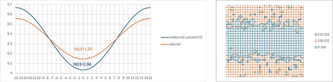
First, we consider the impact of the new blur shape on a simple 15 nm half-pitch image, typically expected for the 5nm node family (including 4nm node).

The first effect to note is the reduction of image contrast mentioned earlier. The normalized image log-slope (NILS) is consequently reduced from 2.84 to 1.85. The reduced contrast also worsened the stochastic influences on the electron density, compared to no blur. The main effect is degradation of the edge definition. There is also increased defectivity in the nominally exposed region, which can lead to shorts between metal lines when negative-tone metal oxide resists are used. This suggests insufficient dose.
The absorbed dose of 20 mJ/cm2 corresponds to 60 mJ/cm2 in 20 nm thick metal oxide resist. A higher dose would lead to increased exposure to the EUV-induced plasma, reducing the resist thickness [7]. This would in turn reduced the absorbed dose used to define the resist pattern, aggravating the stochastic effects.
Example Two: 8 nm Linewidth (16 nm and 32 nm Pitches)
Looking at post-2nm nodes, 8 nm metal half-pitch is specified by the IRDS 2022 edition [6]. A smaller pitch increases the flattening of the sinusoidal optical image, which reduces the contrast further. Figure 3 shows the 8 nm half-pitch, with a larger NILS reduction, and hence, substantially more stochastic defectivity, even affecting the nominally unexposed areas.

A smaller linewidth is also naturally more sensitive to stochastic fluctuations of electron and photon density because NILS is reduced when the linewidth is reduced relative to the pitch. Figure 4 shows this for a 32 nm pitch with the same 8 nm linewidth.

The severe blur-aggravated stochasticity for both 8 nm half-pitch and linewidth means High-NA (0.55 NA) EUV systems cannot support either direct printing or double patterning for the 16 nm pitch, respectively. This goes back to the earlier point that electron blur, not NA, becomes the effective resolution limiter in EUV lithography [8].
References
[1] L. Sun et al., “Review of resist-based flare measurement methods for extreme ultraviolet lithography,” J. Micro/Nanolith. MEMS MOEMS 12, 042001 (2013).
[2] T. A. Brunner et al., “Image contrast metrology for EUV lithography,” Proc. SPIE 12292, 122920A (2022).
[3] D. Schmidt et al., “Characterization of EUV image fading induced by overlay corrections using pattern shift response metrology,” Proc. SPIE 11147, 1114713 (2019).
[4] O. Kostko et al., “Evaluation of Electron Blur for Different Electron Energies,” J. Photopolymer Sci. & Tech. 37, 315 (2024).
[5] Y-H. Huang et al., “A study of hydrogen plasma‑induced charging effect in EUV lithography systems,” Discover Nano 18:22 (2023).
[6] https://irds.ieee.org/editions/2022/irds%E2%84%A2-2022-lithography
[7] F. Chen, Resist Loss Model for the EUV Stochastic Defectivity Cliffs.
[8] F. Chen, Why NA is Not Relevant to Resolution in EUV Lithography.
Thanks for reading Exposing EUV! Subscribe for free to receive new posts and support my work.
Also Read:
Rethinking Multipatterning for 2nm Node
Resist Loss Model for the EUV Stochastic Defectivity Cliffs
Stochastic Effects Blur the Resolution Limit of EUV Lithography
Share this post via:


Chemical Origins of Environmental Modifications to MOR Lithographic Chemistry