

Whether EUV or DUV doesn’t matter at 20 nm pitch
The International Roadmap for Devices and Systems, 2022 Edition, indicates that the “2nm” node due in 2025 (this year) has a minimum (metal) half-pitch of 10 nm [1]. This is, in fact, less than the resolution of a current state-of-the-art EUV system, with a numerical aperture (NA) of 0.33. Even for a next-generation, high-NA (0.55 NA) EUV system, a 20 nm line pitch can only be fundamentally imaged by the basic interference of two plane waves. As Figure 1 shows, the stochastic behavior is expected to be unmanageable, compared to a similarly imaged 80 nm pitch on a state-of-the-art ArF immersion system (Figure 2).
 |
Figure 1. The stochastic appearance (i.e., scattered electron density) of a 10 nm half-pitch image is made worse with 3 nm blur, expected in metal oxide resists [2]. A 20 mJ/cm2 absorbed dose is assumed. The dipole-induced fading is modeled as a + or – 1 nm image shift for either of the two pole’s produced images.
 |
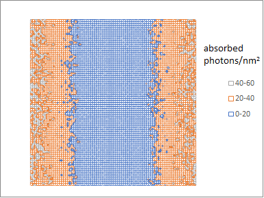
Figure 2. The stochastic appearance (i.e., absorbed photon density) of a 40 nm half-pitch image with ArF dipole illumination is negligible compared to the EUV case of Figure 1, even with a 2 mJ/cm2 absorbed dose assumed. A 6% attenuated phase-shift mask is assumed to be used for negative-tone imaging.
Consequently, double patterning is unavoidable even with EUV lithography. However, any double patterning scheme in EUV lithography for 2nm node still requires the imaging of a 10 nm linewidth, e.g., the cell with four routing tracks and two wide rails (in keeping with TSMC N2 without backside power delivery) shown in Figure 3. Therefore, from what we saw in Figure 1, we still expect a challenged line edge and linewidth definition for the feature size ~ 10 nm.
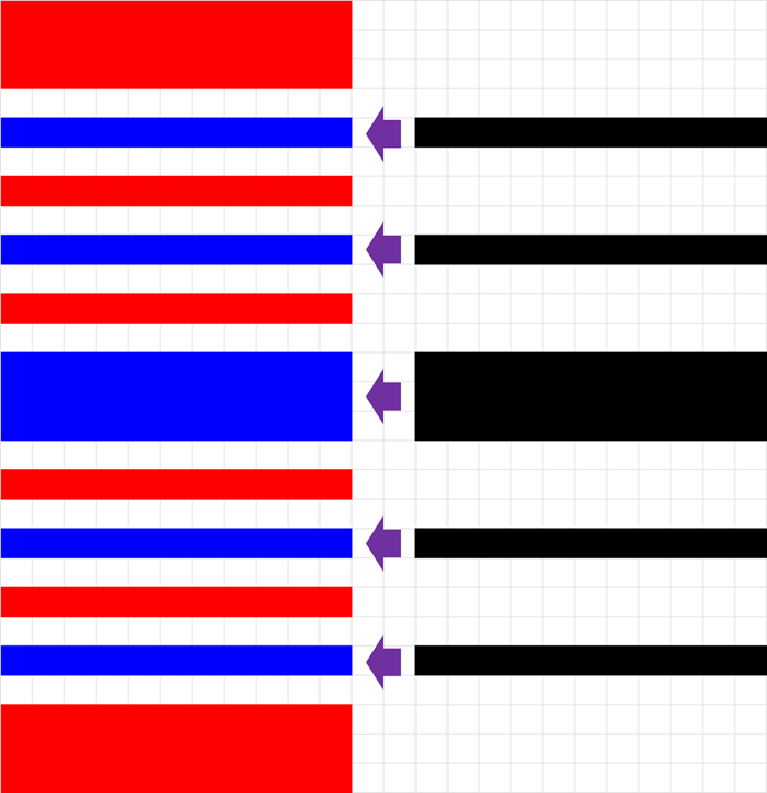 |
Figure 3. A 6-track cell with 10 nm half-pitch features (left) can be formed using double patterning, but a 10 nm linewidth still needs to be formed as the core (right). Note: each square represents 10 nm. The red areas are gaps which are filled after the spacers are formed.
Thus, we expect that the linewidth used in double patterning will itself not be defined by direct exposure but instead by using another double patterning, specifically, self-aligned double patterning (SADP). SADP involves depositing a spacer over the mandrels, etching back to leave only the sidewalls covered, then removing the mandrels. This double the feature density, as there are two sidewall spacers per mandrel (Figure 4).
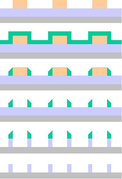 |
Figure 4. Self-Aligned Double Patterning (SADP) doubles feature density by using spacers [3].
In 2021 (prior to 3nm production start), TSMC hinted at this approach in its disclosure in US patent application 20210232747 [4]:
“A method includes forming a first mandrel pattern and a second mandrel pattern. The first mandrel pattern includes at least first and second mandrels for a mandrel-spacer double patterning process. The second mandrel pattern includes at least a third mandrel inserted between the first and second mandrels. The first mandrel pattern and the second mandrel pattern include a same material. The first and second mandrels are merged together with the third mandrel to form a single pattern.”
This is essentially the approach known as LELE-SADP. LELE refers to “Litho-Etch-Litho-Etch”, which would lead to the formation of the two separate mandrel patterns. These mandrel patterns in combination, act as the base pattern, or core pattern, for SADP.
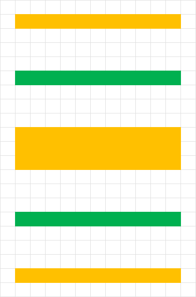 |
Figure 5. LELE is used to generate the black core pattern of Figure 3 (right). The two different colors indicate the two different exposures.
Some of the core pattern linewidths shown in Figure 5 are still too small to be printed directly, so they need to be trimmed from a larger exposed linewidth (Figure 6).
 |
Figure 6. A larger linewidth (left) is trimmed down to give the target 10 nm linewidths (right).
Note, that the trimming cannot be used to get the core pattern in Figure 3, since then the exposed 10 nm gaps would be too narrow (Figure 7).
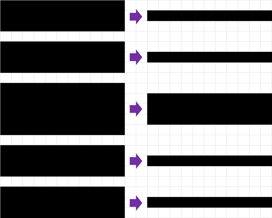 |
Figure 7. Trimming is not feasible here, since the starting 10 nm gaps here (left) are too narrow.
Thus, we see that LELE-SADP is the only option for producing the 6-track cell with four routing tracks and two wide rails, even with EUV. The clincher is, in fact, DUV can produce the exact same 10 nm minimum half-pitch dimensions, with starting exposure pitches of 480 nm. This allows substantial reduction of cost associated with EUV use.
Beyond 2nm
Backside power delivery at the 2nm node and beyond will place the rails at a different layer than the metal routing. This could improve the multipatterning logistics by putting the wide rails and narrow tracks on different layers below and above the transistors, respectively. Thus, a regular grid of minimum pitch lines will suffice for the routing tracks. At 16-18 nm pitch, EUV would be implementing Self-Aligned Quadruple Patterning (SAQP), which would be SADP applied twice successively. DUV would be implementing Self-Aligned Sextuple Patterning (SASP), which would be SADP immediately followed by SATP (Self-Aligned Triple Patterning) [5]. Both EUV SAQP and DUV SASP only require one mask exposure, which will be an improvement over the two masks for LELE-SADP. It is worth noting that SASP takes the resolution of ArF immersion lithography from 38 nm half-pitch down to one-sixth of that, or 6.3 nm half-pitch.
References
[1] https://irds.ieee.org/editions/2022/irds%E2%84%A2-2022-lithography
[2] Z. Belete et al., J. Micro/Nanopattern. Mater. Metrol. 20, 014801 (2021); L. F. Miguez et al., Proc. SPIE 12498, 124980E (2023).
[3] US Patent 5328810, originally assigned to Micron, now expired. https://en.wikipedia.org/wiki/Multiple_patterning#/media/File:Spacer_Patterning.JPG. Creative Commons license CC BY-SA 3.0: https://creativecommons.org/licenses/by-sa/3.0/
[4] Now US Patent 11748540, assigned to TSMC, expires 2035. The scope has been limited to where the third mandrel is shorter than the first and second mandrels.
[5] US Patent 7842601, assigned to Samsung, expires 2029.
Thanks for reading Multiple Patterns! Subscribe for free to receive new posts and support my work.


Intel, Musk, and the Tweet That Launched a 1000 Ships on a Becalmed Sea