High-NA EUV lithography is the anticipated new lithography technology to be introduced for the 2nm node. Essentially, it replaces the 0.33 numerical aperture of current EUV systems with a higher 0.55 numerical aperture (NA). This allows the projection of smaller spot sizes and smaller pitches, roughly 60% smaller compared to 0.33 NA systems. However, the depth of focus of the projected image is limited, due to being inversely proportional to the square of numerical aperture and directly proportional to the square of resolution. A wider numerical aperture leads to a wider range of illumination angles. This, in turn, leads to a larger phase difference from defocus among different spatial frequency components of the image, such as diffraction orders for an array.

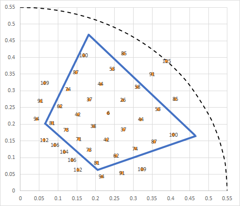
Figure 1. Allowed illumination angles for 28 nm pitch square array, within the first quadrant of the 0.55 NA pupil. The number labels indicate the maximum phase range (in degrees) among the four beams (diffraction orders) making up the image, for a 30 nm defocus. The blue trapezoid outline indicates the zone for minimum 20% pupil fill (5% in one quadrant) to prevent light absorption within the illuminator.
Figure 1 shows the range of phases among the four diffraction orders of a 28 nm square pitch pattern for a 0.55 NA EUV system. The phase range already exceeds 90 degrees, which leads to a maximal intensity change for at least one of the four orders. 30 nm defocus is prohibitive with 20% pupil fill. Resist thickness is therefore expected to be limited to on the order of 20 nm. This leads to an expected absorption of ~10% in organic resists with absorption coefficients of 5/um [1,2]. 0.33 NA systems use resist thicknesses at least twice as thick, allowing absorption of at least ~20%. Thus, the 0.55 NA systems have higher risk of stochastic effects in imaging.

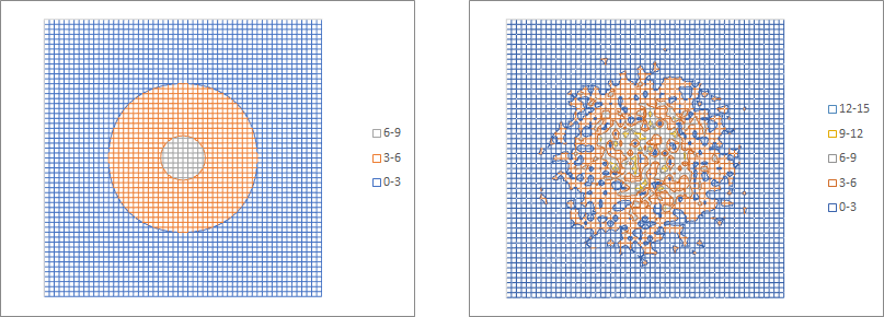
Figure 2. 14 nm dense (28 nm pitch) spot formed as a positive tone darkfield image, assuming 10 mJ/cm2 (absorbed over the whole pitch, >100 mJ/cm2 incident on 20 nm thickness). The nominal image is on the left, while the actual stochastic image is on the right. The numbers indicate the photons absorbed per 0.5 nm x 0.5 nm pixel.
For a 14 nm half-pitch spot in the organic resist case (Figure 2), the absorption outline is rough with very uncertain edge placement, while the interior has numerous areas where no absorption occurs.
Metal oxide resists have absorption coefficients on the order of 20/um (33% absorption in 20 nm thickness) [1,2], so they can provide more photon absorption. However, they are negative tone. That means a bright spot forms a pillar, while a dark spot forms a hole.

Figure 3 14 nm dense (28 nm pitch) spot formed as a negative tone brightfield image, assuming an absorbed dose of 35 mJ/cm2 (>100 mJ/cm2 incident on 20 nm thickness). The nominal image is on the left, while the actual stochastic image is on the right. The numbers indicate the photons absorbed per 0.5 nm x 0.5 nm pixel.
Even for the higher absorbing metal oxide resist (Figure 3), the outline is still very rough and there even appear to be nano-extensions of absorption toward adjacent spots, further blurring the edge. The reason is the lower edge contrast along the horizontal and vertical directions (for 28 nm square array pitch) means stochastic dose fluctuations have a larger opportunity to cross the printing threshold.
0.55 NA EUV imaging therefore requires even higher absorption than 0.33 NA EUV imaging, and this means much more absorptive resists than have already been studied. One other factor not yet considered is electron blur, as increased absorption also means more electrons moving around in the resist. This needs to be covered in a future study.
References
[1] R. Fallica et al., Proc. SPIE 10143, 101430A (2017).
[2] D. De Simone et al., Proc. SPIE 10143, 101430R (2017).
This article first appeared in LinkedIn Pulse: Enhanced Stochastic Imaging in High-NA EUV Lithography
Also Read:
Application-Specific Lithography: Via Separation for 5nm and Beyond
NILS Enhancement with Higher Transmission Phase-Shift Masks
Share this post via:


Musk’s Orbital Compute Vision: TERAFAB and the End of the Terrestrial Data Center