 SAME conference has started with Joel Huloux, Chairman of the MIPI Alliance, who gave a high level introduction about MIPI, rather business than technology oriented, talking to Marketing/Management audience. Extracting the main points from his presentation:
- More than 30 specifications have been issued (Important remark: a MIPI protocols is NOT a standard, like can be PCI Express or SuperSpeed USB)
- About 250 companies are part of the Alliance, that is, the organization can rely on 5000 members (Engineers) to define and write the specifications. That’s a pretty large engineering resource!
- Contributors list includes now the main S/W players, Apple, Google and Microsoft (you can see contributor list below):
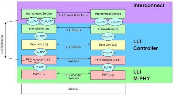
The next presentation, about MIPI Low Latency Interface (LLI), was from Philippe Martin, CTO at Arteris. We already have talked about LLI in Semiwiki in detail, see here, but this technical presentation will certainly provide more precise information to the reader. If we need to summarize, let say that LLI is a packet based, layered communication protocol, including PHY Adapter (PA), Data Link (DLL) and Transaction (TL) layers, for the Controller (the IP sold by Arteris), interfacing with a MIPI M-PHY (PHY IP sold by Synopsys, cosmic Circuits et al.). Any IP need a Verification IP (VIP), isn’t it?
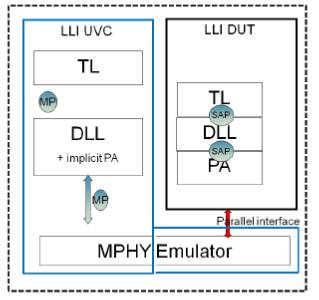
I don’t know if Cadence and Arteris have synchronized, or if these companies are simply addressing hot topics, but this presentation from Gabriele Zarri, MIPI Verification Architect with Cadence, was effectively completing the LLI IP presentation. From an article by Gabriele Zarri that you can read here on Semiwiki, we understand what makes MIPI VIP not so easy to manage is the layered structure of the specification: “…But if this is an easy task with a limited number of parameters in a single-layered protocol, in our example it is not easy to know in advance if a control of the MPHY capabilities is required from a LLI TL, or if a control only on the direct layer beneath him (DLL) will be enough. … It is clear that in a layered verification activity, the only way to guarantee a full coverage is to provide to the users a way of controlling all layers, which makes a VIP user interface extremely complete and therefore complex to create in a easy-to-use manner.”
Before going to listen to Mike Muller, it was time to have a break, and I took the opportunity to meet with Franz Dugand and Ange Aznar, founders of RivieraWaves on their booth. There was a nice demo on the table: their WiFi 11n MAC IP and Modem IP, each loaded in Virtex 6 FPGA (one FPGA per IP as the modem complexity can go up to several million gates depending on the MIMO configuration!) emitting through an external RF to send a movie to a PC, the sound being transmitted by their Bluetooth IP. Impressive and efficient, as it’s always good to have Silicon to show when you want to demonstrate an IP!
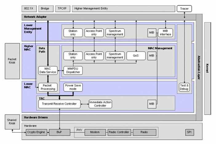
I know Franz and Ange since the time they were working at Wipro, and I am appreciative: when Wipro decided to close the Sophia-Antipolis site, dedicated to wireless IP design and sales, they decided to take the challenge, and started Riviera Waves, focusing on what the market was expecting (in their opinion): Bluetooth (and WiFi) MAC and Modem IP design for low power. It seems that designing for low power was a pretty good idea, as they are not only still alive, but growing! They have written an award winner paper, it can be downloaded here: “Power / Energy Simulation tool for connectivity systems”, getting the Best Paper Award at SAME 2011.

But it’s time now to attend the Keynote talk from Mike Muller, ARM CTO, “A 2020 View & Perspective”. The conference room is now absolutely full, it’s magic to see how just mentioning “ARM” can be efficient. We all felt lucky to listen one of the founders of a company becoming the major threat for Intel, on top of being THE successful IP vendor, and by far!
As many of us, Mike Muller has started to design ASIC, except that this was in 1983-85 and that one chip could be completed by a single man within a year or even less. At that time, he was working for Acorn Computer and the company was selling PC-like, except that the core processor was already a Reduced Instruction Set Computer (RISC), in fact it was the first version, 3000 gates large (!), of the ARM CPU family. VLSI Technology produced the first ARM silicon on 26 April 1985. Then, in 1990, the work was so important that Acorn spun off the design team into a new company called Advanced RISC Machines Ltd, and Mike Muller was part of the founding team. Answering to a question about the attractiveness of engineering career for young people, Mike said that the geek, considered as a sad guy about 10 years ago, is, nowadays, seen as a lot more attractive, as he can make million dollars when successful! That’s certainly true for him, by the way.
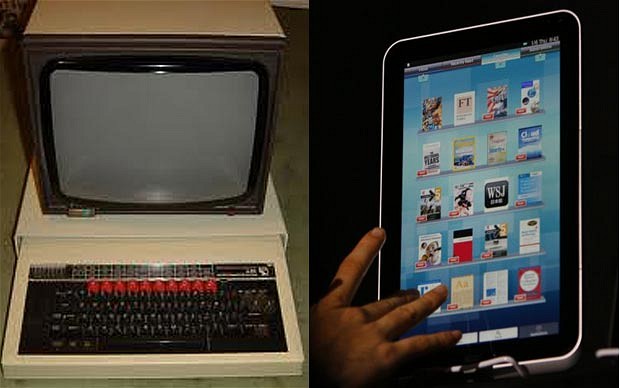
Mike has also shared with us some investigations he has made on the so call “productivity gap”. The results are very interesting! When you compare ARM1 (3K gates), designed in 1985, with Cortex M0 (8K) designed 20 years later, you see that:
- Moore’ law is almost respected, Cortex M0 (designed in 28nm) occupying 1/10,000 of ARM1 area, designed in 2um
- the productivity, expressed in (computing power)/(design effort in man month) has increased more than comparing productivity of S/W development on the same period
- in fact, the most worrying effect comes from the power consumption: if, in term of MIPS, Moore’ law works OK, the power consumption did not decrease, and by far, as it could have done.
A person who has kept in mind all the data related to microprocessor chip design can give you a unique perspective view. In fact, when I say “in mind”, it’s not completely true, as Mike explained us that he had to recover the initial data for ARM1 (layout and paper written specification), back-up on a cartridge, going to University of Cambridge to find a reader, and that he had to manipulate these data quite a bit before being able to exploit it…
I realize that that not so easy to give you the perfect feedback about this presentation. What is missing is the touch of humour that only a British man can give you. As you can see with the syntax in this blog, that’s not the case with me!
By Eric Esteve from IPnest
Share this post via:


Comments
There are no comments yet.
You must register or log in to view/post comments.