The world is abuzz with 3nm and 2nm technology availability. These processes offer the opportunity to pack far more on a single die than ever before. The complex digital systems contemplated will bring new AI algorithms to life and much more. But there is another side of the technology migration story. With all that digital processing comes the need for things like I/Os, sensing, power management and high-speed comms. These are functions delivered by analog IP, and all that must be available on advanced nodes to realize the true monolithic integration opportunity. Analog IP often doesn’t work well at advanced nodes, however. This is a story of how one company isn’t just solving the problem. It is expanding the options at 3nm and beyond to create new paths for new ideas. Read on to see how Analog Bits enables the migration to 3nm and beyond.
The March to 3nm
Analog Bits has a huge catalog of IP that enables all kinds of systems. Billions of units shipped across 1,000+ deliveries since 1995 – an impressive statistic. The company has a long track record of developing critical analog IP across all the top foundries. A little less than two years ago the company was purchased by SEMIFIVE, but the focus and direction of Analog Bits remained the same. You can get more of the backstory on SemiWiki here.
The Analog Bits IP portfolio spans clocking, sensors, I/Os, and SerDes. In the sensor area, on-die LDOs help with power efficiency and power management, a vexing problem for advanced designs. Here is a top-level summary of the portfolio, there is a lot more detail available here.
Clocking
- PCIe clock PHY IP
- High performance C2C PLL
- Digital Core Power PLL
- Wide-range, low power PLL
- Ultra low jitter LC PLL
- Sub-micro watt IOT class PLL
- High reliability radiation tolerant PLL
Sensors
- Digital Core Power
- Bandgap Generator
- System Power Detector
- PVT Sensor
- Power on Reset with Brown-Out Detect
- Power Glitch Detector
- ADC
- LDO
I/Os
- Differential clock TX/RX
- PCIe – HCSL clock drivers
- C2C IO’s Single Ended IO
- Low noise/power crystal oscillators
- Lowest Power OSC pads for IoT
- FPGA class multi-programmable IO
- Voltage tolerant IO buffers
- DDR IO’s
Multi-Rate, Multi-Protocol SERDES
- Lowest power (4pj/bit @ Gen3 & 6pj/bit @ Gen4)
- Low latency – 3/4 UI between parallel and serial Tx/Rx
- Smallest area – 0.1 sq.mm (Gen3) & 0.26 sq.mm (Gen4)
- Programmable for different channel environments
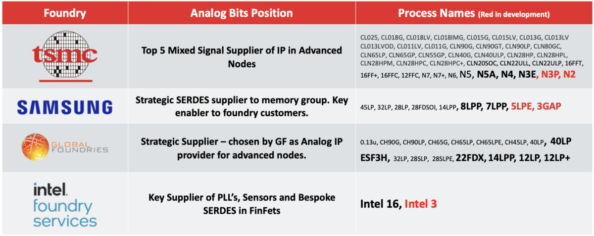
Of course, all this IP must be available on 3nm to facilitate the move to that node, and Analog Bits has a strong story here. The figure below drives home the point. Analog Bits is a critical enabler for 3nm designs.

What’s Next
There is plenty more in the works at Analog Bits beyond 3nm. That detail will be part of future posts. There is one rather key point worth mentioning now, however. Back in 2021, the company announced a novel new, patented IP architecture called Pinless Technology. To minimize power distribution overhead, IP was developed that worked off the core voltage of the chip. This means there is no longer a need to route a different voltage to internal IP since the core voltage is everywhere.
While this style of IP is very useful in 3nm, it takes on a different value at the next node. As we move below 3nm to gate-all-around architectures there will be only one gate oxide thickness available to support the core voltage of the chip. Other oxide thicknesses to support higher voltages are simply no longer available.
In this scenario, the Pinless Technology invented by Analog Bits will become even more critical to migrate below 3nm as all of the pinless IP will work directly from the core voltage. I can’t wait to see how the impact of this innovation shapes the future. And that’s how Analog Bits enables the migration to 3nm and beyond.
Share this post via:


Comments
There are no comments yet.
You must register or log in to view/post comments.