When process nodes reached 28 nm and below, it appeared that design density is reaching a saturation point, hitting the limits of Moore’s law. I was of the opinion that the future of microelectronic physical design was limited to 20 and 14 nm being addressed by technological advances such as FinFETs, double patterning, HKMG (High-k Metal Gate) etc… Probably, this limitation pushed the industry to look at other avenues such as growing vertically giving rise to 3D-IC, also enabling SoC arena, which is of interest today.

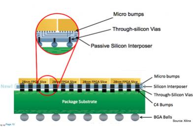
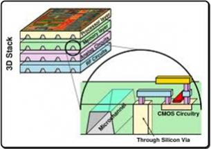
Although the concept of 3D-IC is borrowed from 3D packaging, in the IC world it is definitely an important innovation which unfolds opportunities to go beyond Moore’s law with improved performance and power. Last October, Xilinx announced Virtex-7 2000T which is a 2.5D assembly using silicon interposer and metal interconnect through it to connect four FPGA dies on a single plane; further pushing the industry to actual 3D stacked dies, where multiple dies can be stacked one above the other in different configurations (B2F, F2F, B2B).

3D-IC advantages are aplenty (low power, large memory b/w, high density, high speed etc.) provided the associated challenges (Thermal, EMI, Power management, mechanical stress etc.) are handled well for reliability and planning is done well at the system level. When we talk of 3D, it is like planning for the whole house (all floors) where provisions for interior design have to be considered. Of course there are other challenges like parasitic extraction of TSVs (Through Silicon VIAs) and silicon interposers, physical verification of all dies together with their interconnections and DFT. In this article I am talking about physical design of 3D-IC which needs to be done meticulously to get the optimum result. Following are the steps –
Architecture exploration – This pertains to correct assembly, which needs to be done at the system level where specific die assignment can be done for Analog, Digital, memory, cache and computational modules of a microprocessor. Top level estimation has to be done at this level for optimum assignment to get the best power, speed and density.
Floorplanning – is at the heart of 3D-IC; partitioning at multiple planes including die orientation, TSV placement, keep outs from TSVs (Stress due to TSV can affect threshold voltage of a transistor near it), micro-bumps etc. need to be planned well. For Analog Digital mixed-signal design, proper hand-shake between the two needs to be planned. Thermal effects need to be taken care of and heat sinks need to be planned.
Placement – needs to consider breaking critical paths by adding TSV and using 2[SUP]nd[/SUP] plane to place part of the components. Further, VIAs should be minimized. RF and digital circuitry can be placed separately. TSV placement and micro-bump alignment need to be done.
Routing – needs to consider routing at each plane including backside Redistribution Layers (RDL) and wires connecting through TSVs.
Layout Editing – It goes without mention that editing support for TSVs for all types of interconnections – signal, PG and thermal, micro-bumps and the like is need to be provided. 3D viewing of layout has to be there.
While each tool needs to be extended to 3D capabilities, it also needs to adhere to standards to maintain reliability and interoperability. As the components of a 3D-IC can come from multiple vendors, it is essential that standards need to be defined and adhered for everyone to follow. Although we are late on standards, Standard Development Organizations (3DIC-Alliance, IEEE, JEDEC, SEMI, SI2) are working towards defining these. Exchange Formats for Thermal, Power Delivery Network, Mechanical Stress, Partitioning and Floorplanning and DFT are in the making. Until then, EDA tools in development need to be extensible such that they can adopt the standards later. JEDEC has already released Wide I/O Standard for 3D Memory which was needed since long. It also standardizes for boundary scan test, DRAM test and thermal sensor locations for reliability or memory operations.
3D-IC testing is a large challenge in itself requiring tests at wafer and TSV level in addition to chip level. The industry needs robust test standards to justify the investment in 3D-IC design and manufacturing. We can discuss this separately later.
By Pawan Kumar Fangaria
EDA/Semiconductor professional and Business consultant
Email:Pawan_fangaria@yahoo.com


Intel, Musk, and the Tweet That Launched a 1000 Ships on a Becalmed Sea