Just prior to the opening of the 54[SUP]th[/SUP] Design Automation Conference, Mentor, a Siemens company, and PhoeniX Software issued a press release announcing a new integration between their tools to help designers of photonic ICs (PICs) to close the loop for manufacturing sign-off verification. This is a significant piece of the overall flow puzzle that up till now has been missing. While at the conference, I was able to sit in on a presentation and demonstration to get first impressions of the new flow.
Anyone who has ever taped out a PIC knows it’s prudent to leave time in the schedule to work through a host of false violations seen by foundries trying to use standard CMOS design rule checks for photonics. Curvilinear PIC layouts are particularly challenging for design rule checking (DRC) and logic vs schematic (LVS) applications due to curvilinear shapes represented in GDSII as multi-point polygons.
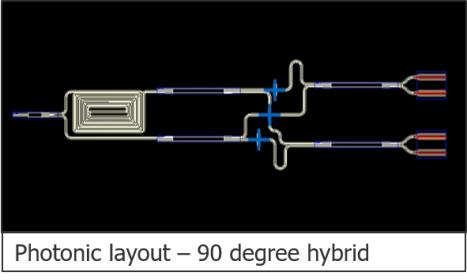
To get a feel for the amount of errors one might have to wade through, Mentor and PhoeniX used a typical photonic layout module known as a 90-degree hybrid used for communications protocols like QPSK. They had Calibre run both a normal CMOS DRC deck and an Equation-based DRC deck on the layout and compared violations found. The results were astounding with 6,420 errors flagged by the regular deck and only 15 flagged by the Equation-based rule deck. The 15 violations found by the equation-based rule deck were real errors. The rest were not. Lest anyone think this is a demo set up to make a point – well, it is – but I can also tell you it is quite indicative of what you would see in real life. Remember this isn’t even a full chip. It’s only a small module or part of a photonics chip.
Foundries are working to upgrade their DRC decks to use more of Calibre’s advanced features such as pattern matching and equation-based design rule checking to reduce the number of false errors flagged. However, even with these changes, the DRC runs are still being done at the foundry right before fabrication which means that real problems are still being found far too late in the design cycle where changes are expensive.
A better solution would be one where the sign-off rule checks could be done incrementally during the design process so that any required circuit changes could be quickly made without having to re-engineer the entire layout. Most PIC design flows today use PhoeniX Software’s OptoDesigner platform for layout synthesis. While OptoDesigner does a great job of correct-by-construction layout, designers are now moving from photonic module development to full blown photonic circuit layout and in that effort, they are cutting corners to create smaller more area-efficient designs which can inevitably cause inadvertent design rule violations.
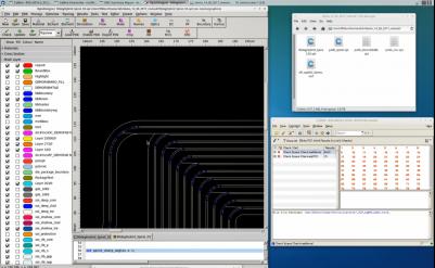
The integration between OptoDesigner and the Calibre nm Platform enables designers to run Calibre verification directly from the OptoDesigner design tool using the Calibre Interactive GUI. Results can then be viewed in OptoDesigner using the Calibre RVE results viewing environment. The Calibre RVE interface enables violation highlighting, zooming, waiver management and error debugging, all while making corrections in OptoDesigner. This was shown live in the demo as the final 15 real errors were quickly changed in OptoDesigner and Calibre was run in real time showing a clean result.
OptoDesigner can also import the Calibre results directly into the tool, if the designer so desires. The interface was developed by PhoeniX Software through Mentor’s OpenDoor program, a mechanism that supports the development, certification, and distribution of interfaces among EDA vendors to promote open interoperability.
The new interface brings some much-needed formalism to the verification of PIC layout for manufacturing design rules. Additional work is underway between the two companies to formalize a better mechanism for photonic LVS. This is still early days for PIC LVS as most PIC designers are still doing the design in a layout tool as opposed to a schematic, but this too is changing as PICs become more complex.
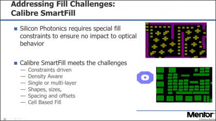
Mentor Calibre is also quite famous for its ability to model manufacturing effects such as Chemical Mechanical Polishing (and the requisite fill patterns needed for it) as well as lithography. These areas look to be natural extensions to the work already done by Mentor and PhoeniX Software. While photonic curvilinear shapes are large in comparison to electronic components, such as FinFet transistors, the performance of the photonics is highly susceptible manufacturing variations such as differences in layer thicknesses and the fidelity of the printed curved shapes.
Calibre SmartFill is Mentor’s tool for handling constraint-driven fill. SmartFill can be used to post-process the design layout to add foundry-specified metal-fill that meets density targets needed to ensure good layer planarity and thickness control while at the same time ensuring that the fill does not impact optical behavior of the photonic circuit.
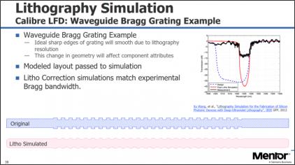
Similarly, Calibre LFD (Litho Friendly Design) is Mentor’s tool for simulating the patterned shapes based on the lithography setup of the foundry. Resulting contours from simulations can be used to analyze the impact of lithography printing effects such as rounding and pinching on the photonic device. Used in conjunction with OptoDesigner, these capabilities would enable designers to adjust the layout prior to tape-out to counter any negative impacts the lithography may have on the design.
All in all, this was a very impressive presentation and demonstration that was well received by those attending the session. It appears that the design flows for integrated photonics are coming together nicely.
See also:
Mentor / PhoeniX Software Press Release
Mentor Calibre nm Platform Product Page
PhoeniX Software OptoDesigner Product Page


Comments
There are no comments yet.
You must register or log in to view/post comments.