The main program for the 70th IEDM opened on Monday morning in San Francisco with an excellent keynote from Dr. Yuh-Jier Mii, Executive Vice President and Co-Chief Operating Officer at TSMC. Dr. Mii joined TSMC in 1994. Since then, he has contributed to the development and manufacturing of advanced CMOS technologies in both fab operations and R&D. In 2022, he received the IEEE Frederik Philips Award recognizing his outstanding accomplishments in the management of research and development. He holds 34 patents globally, including 25 US patents, and holds a B.S. in electrical engineering from National Taiwan University, as well as an M.S. and Ph.D. in Electrical Engineering from the University of California, Los Angeles (UCLA). He treated the audience to a broad view of technology innovation in his keynote. Let’s look at how IEDM opens with a big picture keynote from TSMC’s Yuh-Jier Mii.
About IEDM
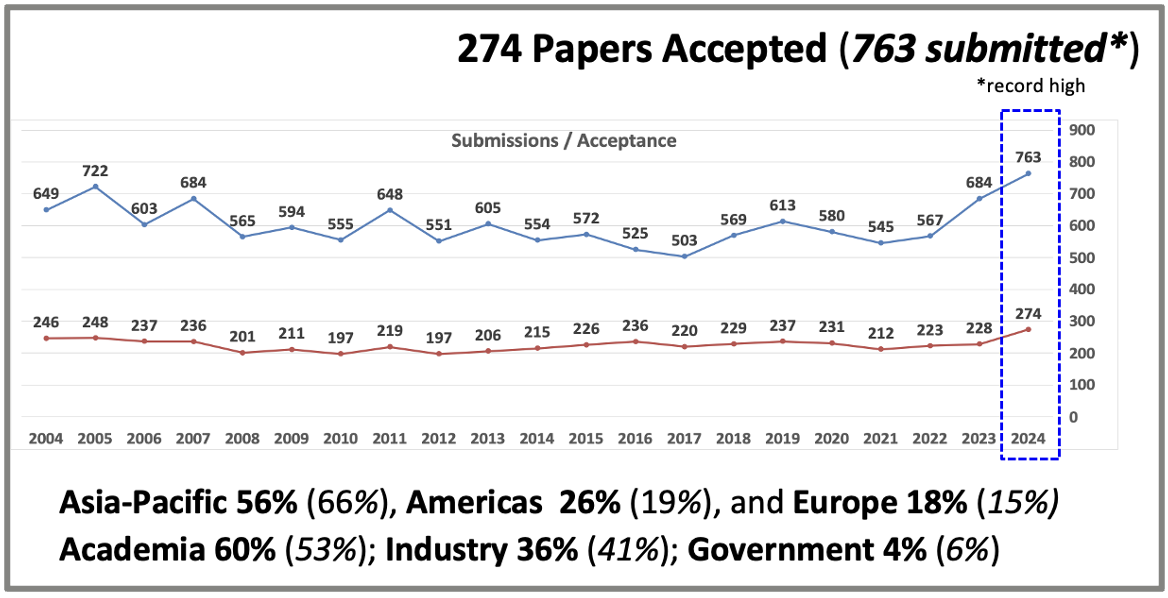
To begin, that wasn’t a typo above. The 70th annual IEEE International Electron Devices Meeting (IEDM) just concluded. This incredibly long-lived conference began tracking technology innovation in the vacuum tube era. For seven decades the event has tracked semiconductor and electronic device technology, design, manufacturing, physics, and modeling. This year’s event had a record high number of submissions at 763 and a record number of accepted papers at 274.
The figure below summarizes the growth of this premier conference over the years.

About the Keynote

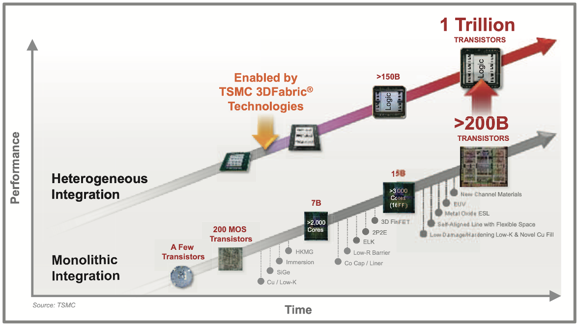
Dr. Mii began his keynote with a short but compelling video that provided an overview of some of the innovations that have occurred in the semiconductor industry in general, and some of the advances contributed by TSMC in particular. All of this is driving the development of a trillion-transistor system in the near future. These trends are summarized in the graphic at the top of this post.
Dr. Mii touched on five key areas in his talk. I will provide a summary of his remarks. He began with a semiconductor industry & market outlook (I). AI is poised to play a key role in the industry’s growth as we move toward one trillion dollars in revenue by 2030. He projected that high-performance computing will contribute 40% of this number, mobile 30%, automotive 15%, and IoT 10%. He discussed the how ubiquitous AI technology is becoming across many products and markets. Generative AI and large language models are contributing to this growth and the complexity of the models for these new applications and the associated training required present substantial new challenges.
He pointed out that these new applications will require gigawatts of power within a few years. Reducing power consumption will be critical to allow these applications to flourish and new device technology and architectural advances will be needed.
Next, Dr. Mii discussed advanced logic technologies (II). He described the industry’s move from planar devices to FinFETs and most recently nanosheet technology for gate-all-around devices at 2nm. Patterning also advanced from immersion lithography to EUV and multi-patterning EUV. Design technology co-optimization, or DTCO has also helped to bring technology to new levels. For example, backside power delivery has helped to reduce power and increase density.
Regarding logic technology frontiers (III), Dr. Mii discussed the evolution from FinFET to nanosheet FET to vertically stacked complimentary or CFET architectures. He explained that the CFET approach holds great promise to allow continued Moore’s Law scaling with its 1.5 – 2X density improvement when compared to nanosheet devices. He described the work going on at TSMC to make CFETs a reality. At this year’s IEDM, TSMC is presenting the first and smallest CFET inverter at a 48nm pitch.
Dr. Mii explained that beyond CFET, the ongoing quest for higher performance and more energy-efficient logic technologies necessitates an accelerated search for channel materials that go beyond those based on silicon. He explained that carbon nanotubes (CNTs) and transition metal dichalcogenides (TMDs) have garnered significant interest due to both their physical and electronic properties. In the area of interconnects, he discussed a new 2D material that is being explored as a superior alternative to copper. This material shows lower thin film resistivity than copper at reduced thicknesses, helping to mitigate line resistance increases in scaled geometries and enhance overall performance.
Dr. Mii then moved to a discussion of system integration technologies (IV). While pushing 2D technology scaling to enable better transistors and higher packing density in monolithically integrated SoCs is important, so are innovations beyond the chip level to extend integration into the heterogenous domain.
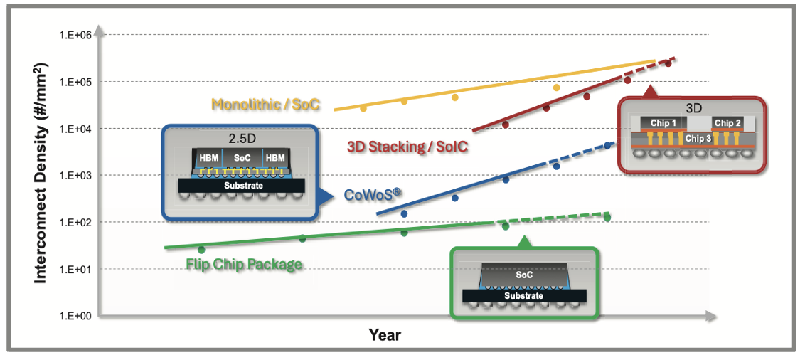
He explained that advanced silicon stacking and packaging technologies, including SoIC, InFO, and CoWoS® continue to aggressively scale down the chip-to-chip interconnect pitch, offering the potential to improve 3D interconnect density by another six orders of magnitude. These trends are summarized in the figure below.

Dr. Mii discussed an emerging System-on-Wafer (SoW) technology, where all the chiplets and HBM memories for an entire system can be integrated directly on a 12-inch wafer. He explained that this approach can deliver an additional 40X compute improvement when compared to the most advanced data center AI accelerator today. Optical interconnect was also discussed, which can provide 20X more power efficiency than copper interconnect. Vertical stacking of logic and optical transceivers will help deliver these improvements. He explained that today the laser light source is outside the chip, but efforts are underway to integrate the laser on chip as well.
Dr. Mii concluded with a discussion of specialty technologies (V). Many of the items discussed here are high frequency or analog in nature to accommodate the interface between the digital and analog (real) world. He discussed innovations spanning N16 to N4 to accommodate the increased demands of new standards for WiFi.
Advances in embedded non-volatile RAM were also discussed in this part of the keynote. The benefits and challenges of both MRAM and RRAM were covered. CMOS image sensors were also discussed. This is a critical technology for automotive applications. As pixel size decreases, new approaches are needed to maintain sensitivity and dynamic range. Dr. Mii described work to separate the photo diode from the pixel device and re-integrate them using 3D wafer-to-wafer stacking.
Summary
Dr. Mii concluded by observing that semiconductor innovations, encompassing advances in device technology, system-level scaling, and customer-specific design ecosystems will remain pivotal in driving rapid technological progress in the era of AI. He pointed out that TSMC is actively exploring a new array of innovations for future generations of technology, system integration platforms, and design ecosystems. These efforts will be crucial in meeting the increasing societal demands for energy-efficient, data-intensive computing in the coming decades. He invited the audience to join in this important collaboration. And that’s how IEDM opens with a big picture keynote from TSMC’s Yuh-Jier Mii.
Also Read:
Analog Bits Builds a Road to the Future at TSMC OIP
Maximizing 3DIC Design Productivity with 3DBlox: A Look at TSMC’s Progress and Innovations in 2024
Synopsys and TSMC Pave the Path for Trillion-Transistor AI and Multi-Die Chip Design


Comments
One Reply to “IEDM Opens with a Big Picture Keynote from TSMC’s Yuh-Jier Mii”
You must register or log in to view/post comments.