The TSMC Open Innovation Platform (OIP) event brings together a wide array of companies reporting cutting edge work that are part of TSMC’s rather substantial ecosystem. The event covers everything from high-performance computing to mobile, automotive, IoT, RF and 3D IC design. Of particular interest for this post is a presentation made by Alchip. At the current incredible pace of innovation, methods to extend and enhance Moore’s law are of great interest to many. At the event, Alchip reveals how to extend Moore’s law with a targeted combination of technology and know-how. Read on to learn more.

The presentation was given by James Huang, vice president of R&D at Alchip Technologies. James began his presentation describing the yield challenges associated with a very large die at advanced technology nodes. As die size increases, yield decreases, sometimes approaching single-digit numbers. An alternative approach to address this issue is to segment the design into smaller portions, or chiplets and integrate the resulting pieces with advanced interface and packaging technology. A group of smaller chips, or chiplets will deliver a yield far better than a single, large die as shown in the figure.
James pointed out this approach does introduce additional costs from the advanced package, die to die interfaces and higher testing costs. The approach still delivers competitive total cost in many cases, however. There are several key ingredients required to make this approach viable. They include:
- 2.5/3D packaging technology: TSMC 3DFabric™ & CoWoS® makes high bandwidth memory multi-die integration feasible.
- Die-to-die communication: Alchip APLink (Advanced Package Link) D2D IOs enables high-speed data traffic between multiple chiplets.
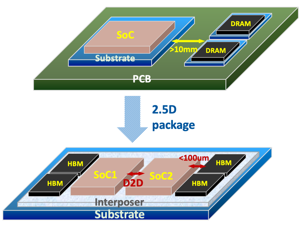
James explained that Alchip’s APLink 4.0 is compatible with TSMC’s N3 process and offers a 16 Gbps line rate. It can use TSMC’s most advanced CoWos technology, offering five metal layers. An approach like this can definitely cut the large die yield issue down to size. This method of chip decomposition and reintegration is illustrated in the figure below.

He provided some information about APLink 4.0. Key features include:
- Source-synchronous I/O bus running with standard core voltage
- 12Tbps per PHY macro
- 16Gbps per DQ line
- 25+ pJ/bit
- 5ns latency
- Reliable system operation
- De-skew, DBI
- Eye training & monitoring
- Lane repair
- PVT monitoring
The APLink IP is delivered as a hard PHY macro with a soft controller. The IP supports south/north and east/west orientations. Symmetric PHY alignment achieves minimum die-to-die wire length. James then discussed the steps required to develop an effective chiplet-based design approach. Items to consider include:
- Fundamentals
- Process node selection for each chiplet
- D2D IP performance and readiness
- 5D/3D packaging lengthens the design cycle and introduces new risks
- Total design and manufacturing cost
- System architecture considerations
- How to distribute sub-systems across multiple chiplets (chiplet partitioning)
- Are power distribution networks sufficient?
- Timing, thermal and SI/PI budgeting
- Can individual chiplets be shut off?
As you can see, there is a lot to consider. James went on to point out other considerations, such as thermal dissipation, mechanical stress and warpage, and overall routing space for the interfaces. A lot of these issues must be considered early in the design process. These problems can be tamed, however. A successful 2.5D design was showcased during his presentation that contained multiple chiplets and HBM memory stacks.
He also discussed strategies for energy management for complex chiplet-based designs, as well as signal and power integrity considerations. Testing strategies for this kind of design were also discussed. Test can be quite a bit more complex when compared to a monolithic design.
James concluded with an overview of Alchip’s customer engagement model. The company works with the customer at every step in a collaborative way to ensure project success. If you are considering a chiplet-based approach for your next design, you should carefully consider your ASIC partner. There are many challenges with this type of design, and James demonstrated in his presentation a strong command of the requirements needed to achieve success.
You can learn more at www.alchip.com. You can also get lots of good information about Alchip on SemiWiki here, including a copy of the press release about the TSMC OIP presentation. And that is the story of how Alchip reveals how to extend Moore’s law with a targeted combination of technology and know-how.
Also Read:
Alchip is Painting a Bright Future for the ASIC Market
Maximizing ASIC Performance through Post-GDSII Backend Services
Alchip at TSMC OIP – Reticle Size Design and Chiplet Capabilities
Share this post via:


Comments
There are no comments yet.
You must register or log in to view/post comments.