You are currently viewing SemiWiki as a guest which gives you limited access to the site. To view blog comments and experience other SemiWiki features you must be a registered member. Registration is fast, simple, and absolutely free so please,
join our community today!
            WP_Term Object
(
    [term_id] => 14
    [name] => Synopsys
    [slug] => synopsys
    [term_group] => 0
    [term_taxonomy_id] => 14
    [taxonomy] => category
    [description] =>
    [parent] => 157
    [count] => 755
    [filter] => raw
    [cat_ID] => 14
    [category_count] => 755
    [category_description] =>
    [cat_name] => Synopsys
    [category_nicename] => synopsys
    [category_parent] => 157
    [is_post] =>
)

WP_Term Object
(
    [term_id] => 14
    [name] => Synopsys
    [slug] => synopsys
    [term_group] => 0
    [term_taxonomy_id] => 14
    [taxonomy] => category
    [description] =>
    [parent] => 157
    [count] => 755
    [filter] => raw
    [cat_ID] => 14
    [category_count] => 755
    [category_description] =>
    [cat_name] => Synopsys
    [category_nicename] => synopsys
    [category_parent] => 157
    [is_post] =>
)
Once upon a time, designing a product with a first generation SoC on board, we were trying to use two different I/O peripherals simultaneously. Seemed simple enough, but things just flat out didn’t work. After days spent on RTFM (re-reading the fine manual), we found ourselves at the absolute last resort: ask our FAE.
After about… Read More
There’s never a dull moment in the foundry race to offer FinFET processes that enable leading-edge SoC design. Today I attended a webinar hosted by Samsung and Synopsys on how to enable 14nm FinFET design. The two speakers were Dr. Kuang-Kuo Lin from Samsung and Dr. Henry Sheng from Synopsys.
Dr. Kuang-Kuo Lin, Samsung
Dr.… Read More
Funny story, @ #49DAC I saw Aart with a very relaxed look on his face looking at the exhibit hall and in my mind he was thinking, “Mine, all mine!” But I digress……. Synopsys is the #1 EDA company for a reason and here is the supporting data for that hypothesis:
Synopsys is committed to accelerating Innovation… Read More
Designing at the 20nm node is harder than at 28nm, mostly because of the lithography and process variability challenges that in turn require changes to EDA tools and mask making. The attraction of 20nm design is realizing SoCs with 20 billion transistors. Saleem Haider from Synopsys spoke with me last week to review how Synopsys… Read More
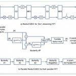
A basic building block of any communication system today is the fast Fourier transform, or FFT. A big advantage of FPGA implementations of FFTs is they can be scaled and tuned for the task at hand, optimizing data flow, resource use, and power consumption. Scaled, that is, up to the clock speed of the FPGA – or so it would seem.
Today’s… Read More
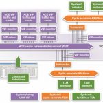
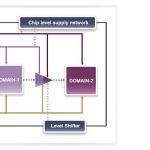
The burgeoning need of high density of electronic content on a single chip, thereby necessitating critical PPA (Power, Performance, Area) optimization, has pushed the technology node below 0.1 micron where static power becomes equally relevant as dynamic power. Moreover, multiple power rails run through the circuit at different… Read More
Cliff Hou of TSMC gave the keynote today at SNUG on Collaborate to Innovate: a Foundry’s Perspective. Starting around 45nm the way that a foundry has to work with its ecosystem fundamentally changed. Up until then, each process generation was similar enough to the previous one, apart obviously from size, that it could be … Read More
Will 14nm Yield?by Daniel Nenni on 03-26-2013 at 9:00 pmCategories: EDA, Synopsys
If I had a nickel for every time I heard the term “FinFET” at the 2013 SNUG (Synopsys User Group) Conference I could buy a dozen Venti Carmel Frappuccinos at Starbucks (my daughter’s favorite treat). In the keynote, Aart de Geus said FinFET 14 times and posed the question: Will FinFETs Yield at 14nm? So that was my mission, ask everybody… Read More
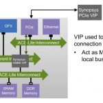
So, you dropped that piece of complex IP you just licensed into an SoC design, and now it is time to fire up the simulator. How do you verify that it actually works in your design? If you didn’t get verification IP (VIP) with the functional IP, it might be a really long day.
Compliance checking something like a PCIe interface block is a … Read More
I was at SNUG earlier today at both Aart’s keynote that opened the conference and at his “meet the press” Q&A just before lunch. The keynote was entitled Bridges to the Gigascale Decade. And the presentation certainly contained lots of photos of bridges! Anyway, I’m going to focus on just one thing,… Read More