Synopsys has long been known for its leading position in the digital logic synthesis world. More recently however, the company started delving into the world of photonic integrated circuit (PIC) design. Synopsys started down this path from the system level with a 2010 acquisition of Optical Research Associates and their CODE V and LightTools products. These products deal with discrete optical components and free-space optics. They then moved down into the photonic IC level with a 2012 acquisition of RSoft Design Group that brought with them several very good photonic simulation engines.
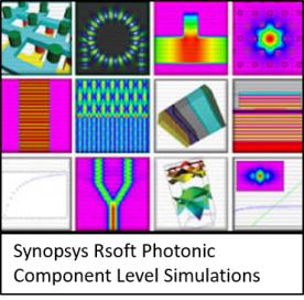
The RSoft group, now part of Synopsys’ Optical Solutions Group, brought with it simulation tools at both the system and component levels. At the component level, these tools are very much like what Synopsys offers for electronic technology CAD (TCAD). Their offerings include tools for mode solving, beam propagation (BPM and FDTD) and modeling for diffraction elements, gratings and active devices like lasers, to name a few.
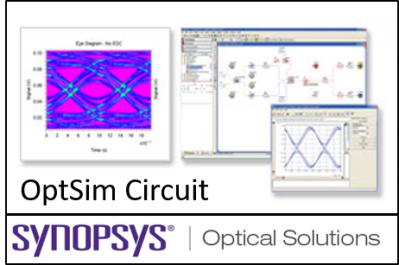
At the system level, RSoft brought into Synopsys a simulator called OptSim. OptSim is well known in the photonics industry and was historically focused on telecommunications systems and datacom applications. Synopsys continues to sell this software and has also augmented the platform and pushed it into the PIC world with release of OptSim Circuit. OptSim Circuit is, as its name implies, a circuit level simulation environment for PICs.
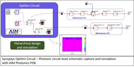
I say environment because, like its predecessor OptSim, OptSim Circuit brings with it all the features you need to easily capture and simulate a PIC design. OptSim Circuit uses an easy-to-learn drag and drop schematic capture environment that features hierarchy and a library of parameterized high-level photonic building blocks that can be used to create a circuit. The platform enables designers to model at different levels of abstraction and then verify the functional implementation against system models used during system level simulations.
OptSim Circuit includes the ability to easily set up complex test benches for multiple what-if scenarios and allows designers to run sweeps through parameter ranges and to check for impacts of process variations on critical design parameters. The software also enables visualization of simulation outputs in terms familiar to system designers such as eye diagrams, BER, FSR, etc.
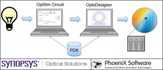
More recently, Synopsys completed a PDA Flow link with PhoeniX Software to enable a bridge between the system- and circuit-level functional PIC design and an implementation of the design targeted to a specific foundry and packaging technology. PhoeniX Software specializes in PIC design layout tools. Their product, OptoDesigner, also uses PDKs and a library of high-level parameterized photonic building blocks. Using the PDA Flow link, PhoeniX can take the circuit from OptSim Circuit and synthesize a foundry-specific DRC correct layout that matches the design intent as described by the designer in OptSim Circuit.
Synopsys and PhoeniX will be jointly demonstrating this new flow at the Optical Fiber Conference (OFC) in Los Angeles in a couple of weeks. The demo will be given at the Synopsys booth #2519 on March 21[SUP]st[/SUP] and 22[SUP]nd[/SUP] from 10:00a to 12:00p and 2:00p to 4:00p, respectively. A feature of this demo is that they will be using the AIM Photonics PDK to show that this flow can in fact be used to create designs that can be fabricated now on MPW runs using the AIM Photonics silicon and silicon nitride processes.
Synopsys and PhoeniX have also completed work with the LioniX foundry in Europe to support this same flow with the LioniX Triplex (silicon nitride) technology.
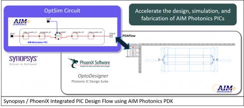
While this flow is similar to what is done in the electronic world between capture/simulation and place and route, it is also very different. The differences come from the fact that the waveguides that connect photonic components are not simple connectors. With the right conditions, waveguides can actually become components in their own right that dramatically affect the signal. They can even be used to modulate the signal depending on how they are built. Given this phenomena, the photonics schematic takes on a much larger role than in electronics, in that the designer needs to comprehend some of these layout affects even while working in an abstract schematic.
The flow between Synopsys and PhoeniX enables this by allowing the designer to capture schematic connections as a combination of waveguide segments. These segments can be modeled and simulated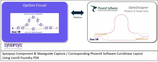 with the rest of the circuit to allow the designer to ensure correct functionality. The segmented connections are then passed on to the PhoeniX layout tools through the PDA link, where they are synthesized per the parameters in the schematics. Placement of components and waveguide segments are accomplished by the PhoeniX tools based on the relative placements of components and waveguide segments in the schematic. PhoeniX uses something called elastic-connectors along with the relative placement information of components and waveguide segments to enable the physical placement and routing of the waveguides to meet the designer’s intent.
If you are curious to see how this all works, Synopsys and PhoeniX encourage you to stop by the Synopsys booth at OFC at the appointed times.
See also:
Synopsys RSoft Products Web Page
Synopsys / PhoeniX PDA Link Flow


Comments
There are no comments yet.
You must register or log in to view/post comments.