The traditional batch-oriented DRC process run as a final check to ensure compliance with foundry yield goals is quickly moving toward a concurrent DRC process performed early and often throughout design, especially at the 28 nm and smaller process nodes. What are the technology factors causing this change?
- Increasing number of rules and their complexity
- Coloring – the multi-pattern mask requirements
- Metal fill is more complex and impacts timing results
- Place and Route (P&R) has to be concurrent with DRC to get closure
FinFET transistors starting at the 22 nm node added some complexity to the DRC process, however the double patterning technology (DPT) required at 20 nm caused more computational complexity than FinFET for DRC jobs. Having to comply with 1,000 design rules at 10 nm does not look fun to me. Finally, keeping the CMOS process planar by adding fill patterns has mushroomed in effort required.
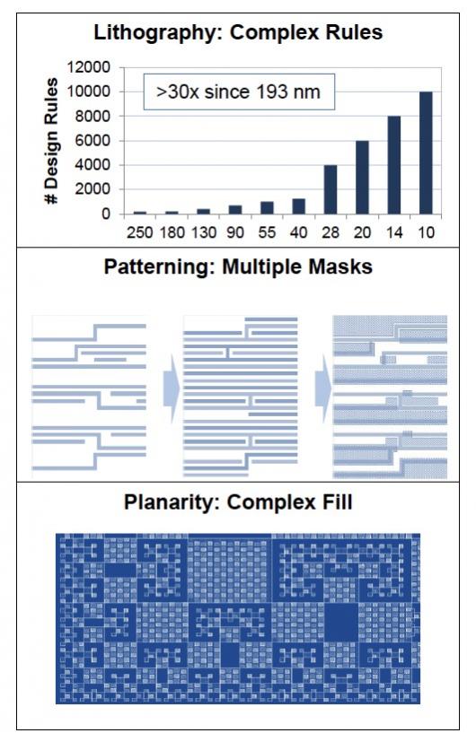
DRC Challenges
Related – FinFETs for your Next SoC
DRC tools can identify and automatically fix odd-cycle loops found with DPT, but when we start using Triple Patterning at the 10 nm node you will initially just get a warning and have to make the fixes yourself.
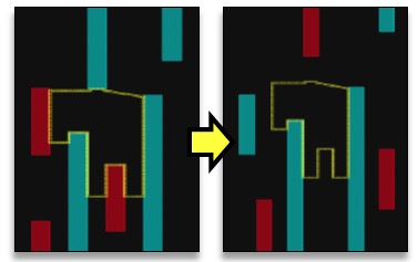
DPT Auto Repair
The computational effort required on verifying the coloring on triple patterning is increasing, so changing the approach to include heuristics is one way to keep run times down. There could even be quad patterning required for the 7 nm node.
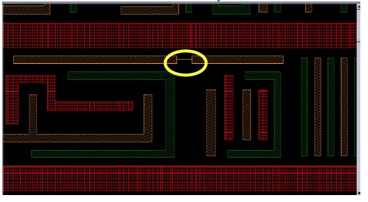
Triple Patterning coloring conflict
Metal fill insertion now has to deal with coloring, alignment with signal direction, uni-directional track-based fill and balancing out the density to avoid large gradients:
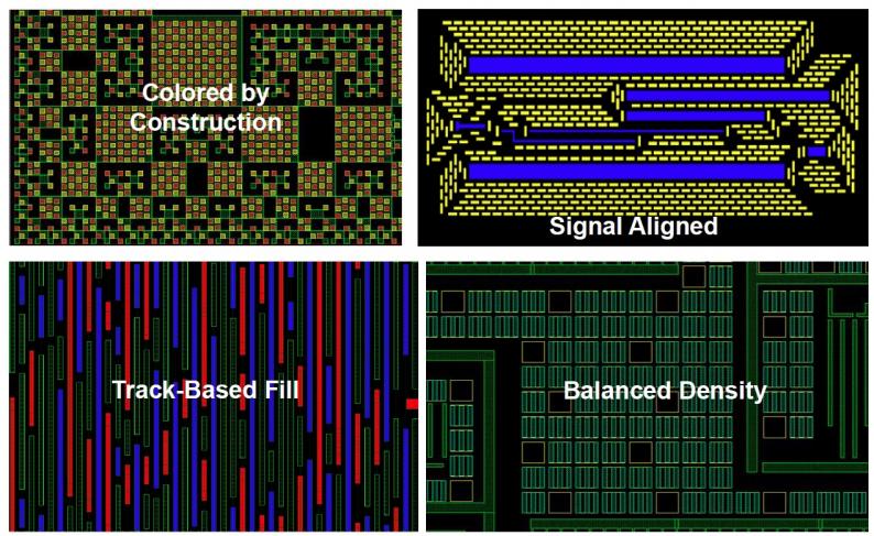
Metal Fill Insertion
A side effect of adding metal fill is that it adds extra capacitors, thus affecting the timing on nearby nets. Metal fill always degrades Worst-case Negative Slack (WNS) and Total Negative Slack (TNS), causing iterations to get timing fixed. A smart approach is to identify these effects early, fixing them prior to tape out by mitigating the effect.
Related – Challenges of 20 nm IC Design
The latest DRC tool from Synopsysis called IC Validator and it has features to address each of the new challenges talked about so far. Concurrent DRC during P&R is called In-Design, saving you on turn around time.
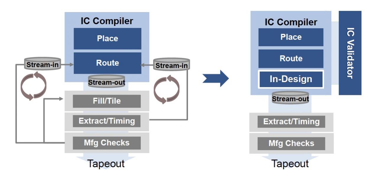
Traditional vs In-Design Flows
Starting at the 28 nm node is where you see the biggest benefit of using In-Design instead of the older, iterative flow. Something like 20 of the top 25 IC Compiler customers are already using In-Design. Have a single database between IC Compiler and IC Validator means that there is no data streaming, tool setup or translation steps required. IC Validator runs natively incremental on just the changed areas, saving more time over tools that are forced to run on the whole IC layout. One Synopsys customer used the automatic DRC repair feature on their 28 nm design and actually saved 2 weeks in their schedule.
Many of the DPT errors that are identified can be automatically repaired, and the router is part of making the needed repairs. This tight integration between P&R and DRC is really needed to cut down iteration times.
Related – Enabling 14 nm FinFET Design
Critical nets can meet their timing requirements by having the metal fill insertion add spacing on the same layer, which lowers the parasitic capacitance values.
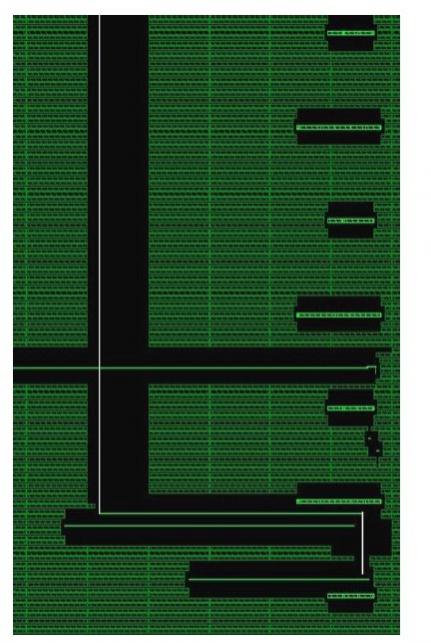
Critical nets with metal fill spacing
IC designers can be somewhat sheltered from coloring and fill, but to get the best chip performance they may adopt a DRC methodology that is concurrent with P&R, run early and often. Using IC Validator is straight forward because the leading foundries (TSMC, UMC, SMIC) and Intel Custom Foundry all support the run sets for their process nodes. You can even work with the FD-SOI process at 28 nm from ST today, and smaller nodes coming soon.
Share this post via:


Comments
There are no comments yet.
You must register or log in to view/post comments.